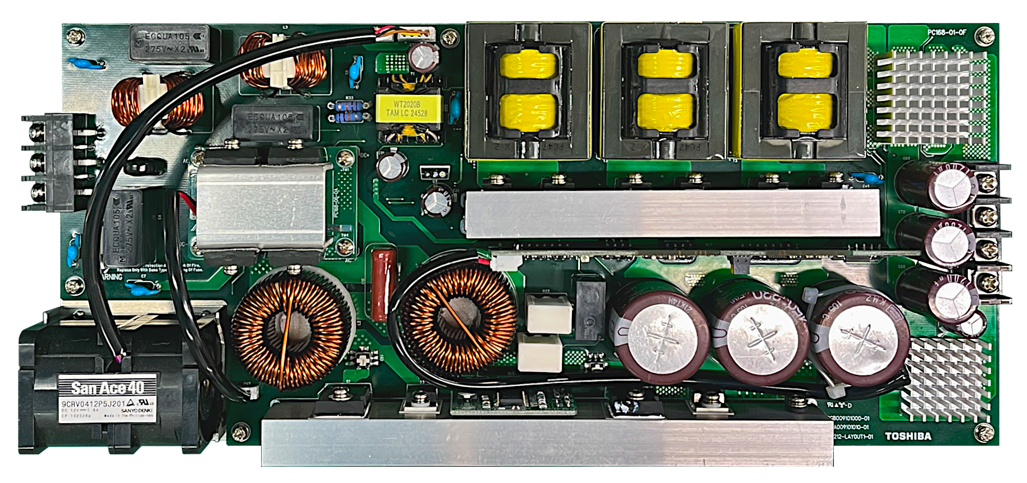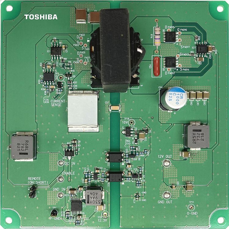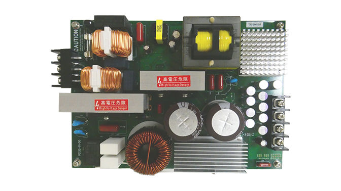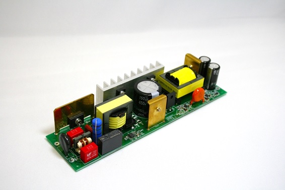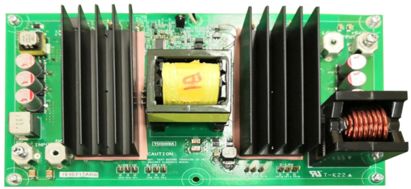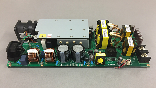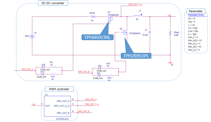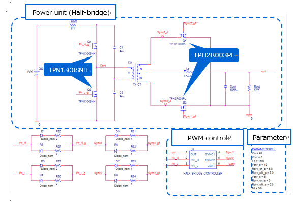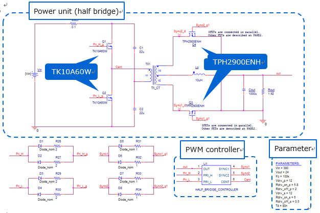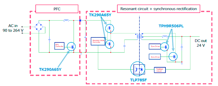
MOSFET
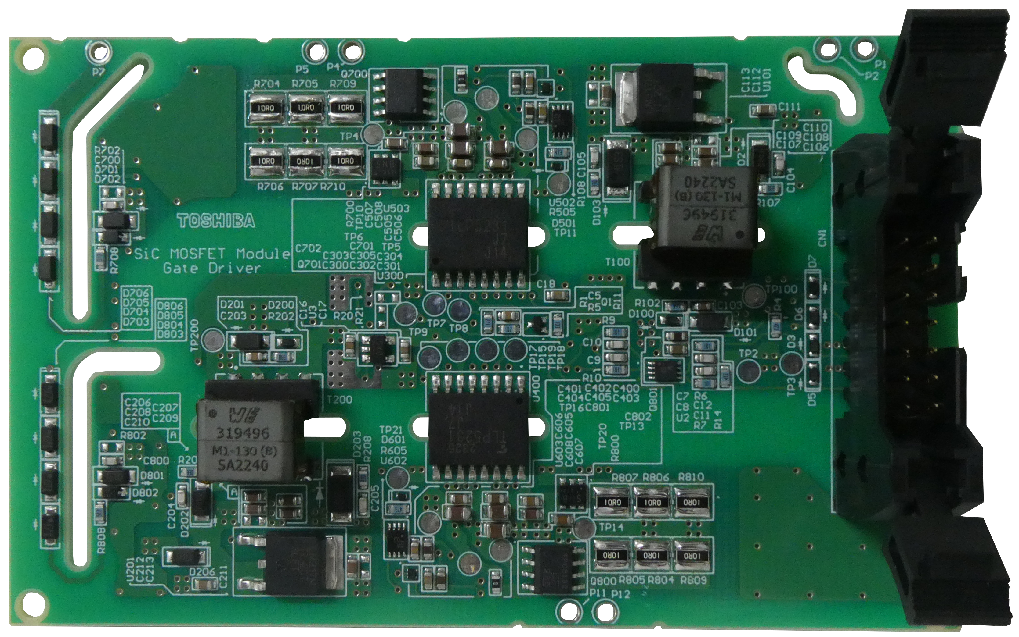
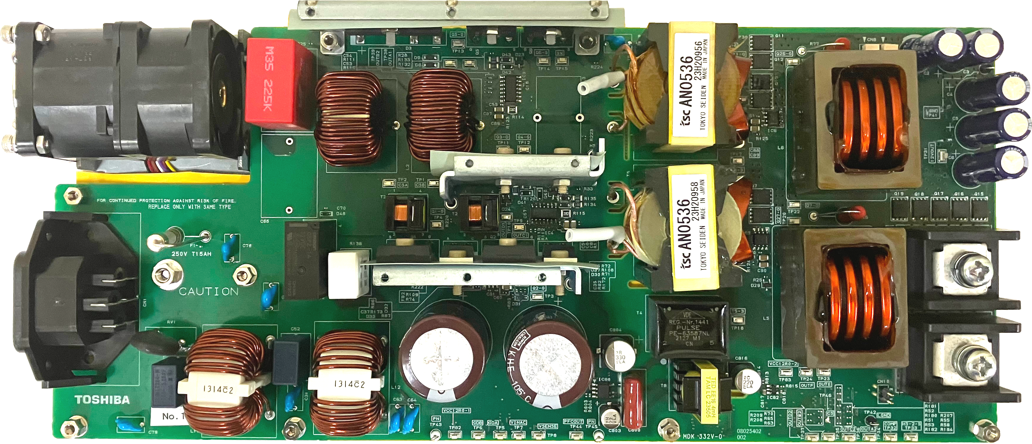
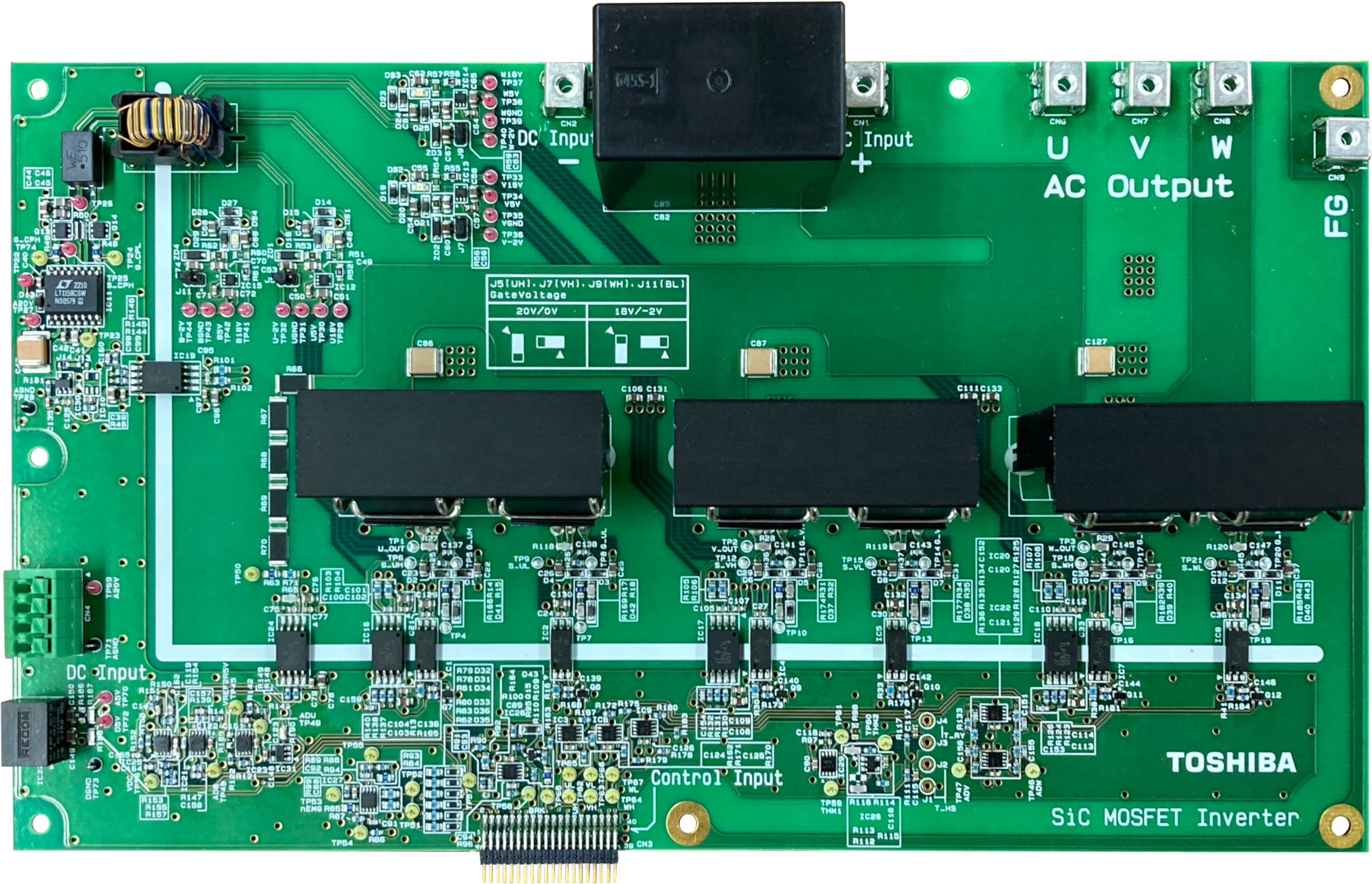
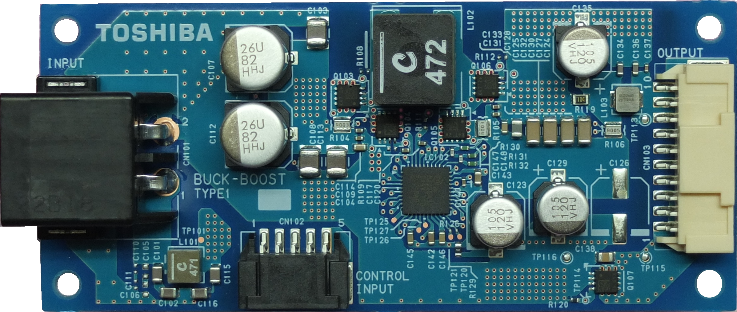
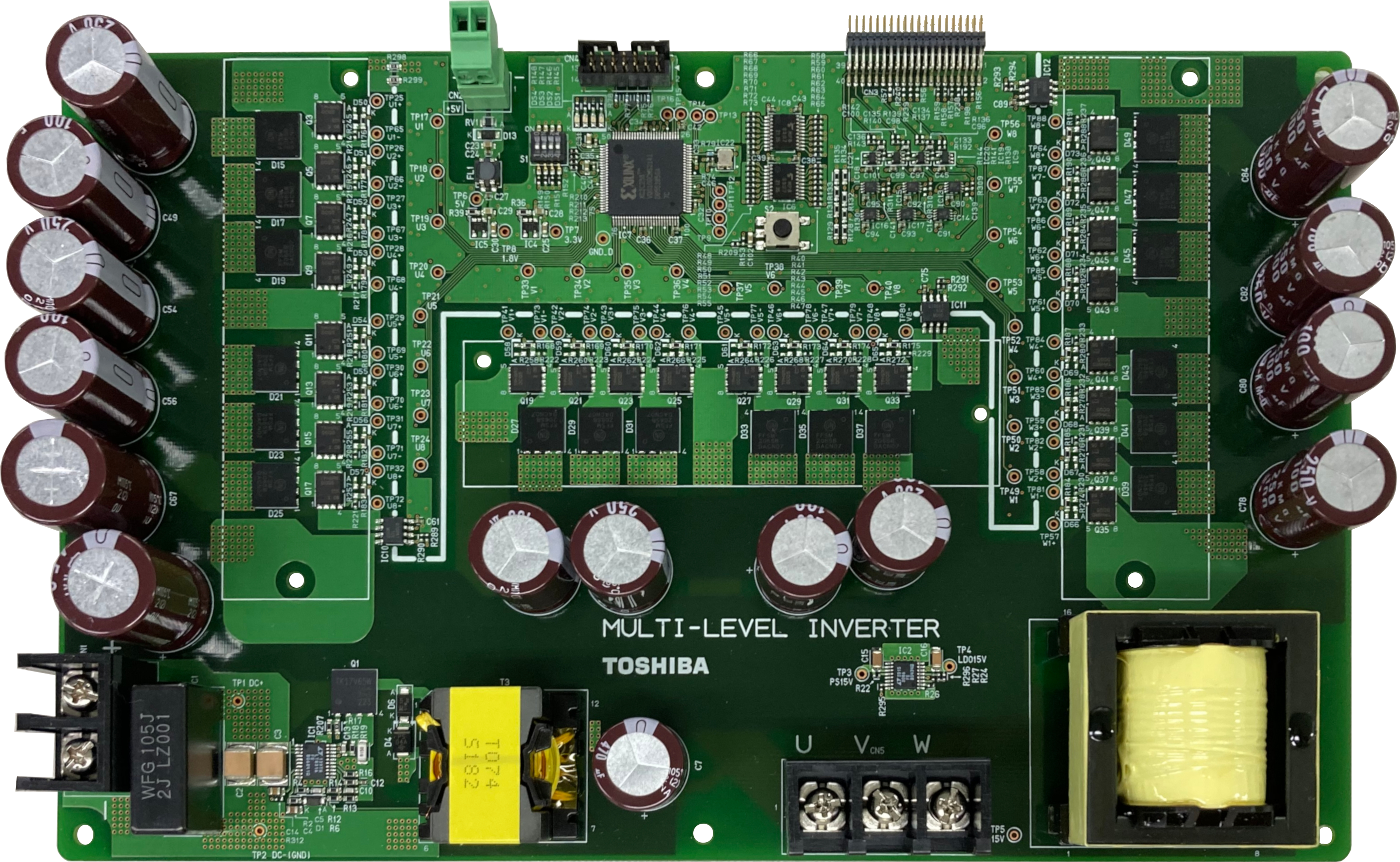
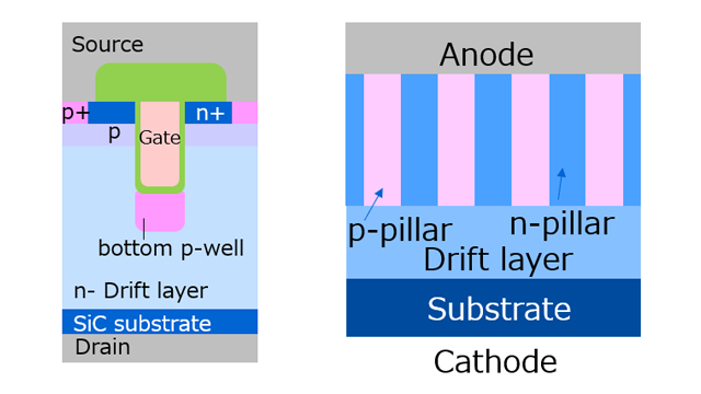
MOSFET是一种场效应晶体管(利用电场控制电流),由金属氧化物半导体制成,是目前使用最广泛的生产技术。在功率MOSFET领域,碳化硅(SiC)也被使用,因为它是电源、逆变器和其他应用所需的更高性能和效率的理想选择。东芝多年来一直致力于MOSFET的开发和生产,我们广泛的低中高耐压设备产品线具有低损耗、高速度、低导通电阻和小封装等特点—适合各种应用的MOSFET。
产品线
您可以通过选择规格来缩小适用产品的搜索范围。
您可以按包装类型或引脚数量缩小适用产品的搜索范围。


- TCSP6A-172101
-
Package Size
W : 2.14 mm 0.084 inch L : 1.67 mm 0.066 inch H : 0.11 mm 0.0043 inch

- SOT-1118 (UDFN6)
-
Package Size
W : 2.0 mm 0.079 inch L : 2.0 mm 0.079 inch H : 0.75 mm 0.030 inch
.png)
- SOT-1220 (DFN2020B(WF))
-
Package Size
W : 2.0 mm 0.079 inch L : 2.0 mm 0.079 inch H : 0.6 mm 0.024 inch

- SOT-1220 (UDFN6B)
-
Package Size
W : 2.0 mm 0.079 inch L : 2.0 mm 0.079 inch H : 0.75 mm 0.030 inch


.png)

L.png)
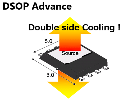
- DSOP Advance(WF)L
-
Package Size
W : 5.0 mm 0.20 inch L : 6.0 mm 0.24 inch H : 0.76 mm 0.030 inch
M.png)
- DSOP Advance(WF)M
-
Package Size
W : 5.0 mm 0.20 inch L : 6.0 mm 0.24 inch H : 0.76 mm 0.030 inch

.png)
.png)
.png)


- TCSPAC-153001
-
Package Size
W : 2.98 mm 0.12 inch L : 1.49 mm 0.059 inch H : 0.11 mm 0.0043 inch

- TCSPAG-341501
-
Package Size
W : 3.37 mm 0.13 inch L : 1.47 mm 0.058 inch H : 0.11 mm 0.0043 inch


.png)

.png)

.png)
All package dimensions are guaranteed in millimeters as mentioned on datasheet. Package dimension in inches is round to 2 significant digits converted with 1mm=0.0393701inch.
请输入3个以上字符
About information presented in this cross reference
The information presented in this cross reference is based on TOSHIBA's selection criteria and should be treated as a suggestion only. Please carefully review the latest versions of all relevant information on the TOSHIBA products, including without limitation data sheets and validate all operating parameters of the TOSHIBA products to ensure that the suggested TOSHIBA products are truly compatible with your design and application.Please note that this cross reference is based on TOSHIBA's estimate of compatibility with other manufacturers' products, based on other manufacturers' published data, at the time the data was collected.TOSHIBA is not responsible for any incorrect or incomplete information. Information is subject to change at any time without notice.


文档
技术专辑

参考设计