


- 型号 & 关键词搜索
- 交叉搜索
- 参数搜索
- 库存查询与购买
This webpage doesn't work with Internet Explorer. Please use the latest version of Google Chrome, Microsoft Edge, Mozilla Firefox or Safari.
请输入3个以上字符 Search for multiple part numbers fromhere.
The information presented in this cross reference is based on TOSHIBA's selection criteria and should be treated as a suggestion only. Please carefully review the latest versions of all relevant information on the TOSHIBA products, including without limitation data sheets and validate all operating parameters of the TOSHIBA products to ensure that the suggested TOSHIBA products are truly compatible with your design and application.Please note that this cross reference is based on TOSHIBA's estimate of compatibility with other manufacturers' products, based on other manufacturers' published data, at the time the data was collected.TOSHIBA is not responsible for any incorrect or incomplete information. Information is subject to change at any time without notice.
请输入3个以上字符
DTMOSⅥ 600V N沟道功率MOSFET采用TO-247-4L(X)封装,有助于提高工业设备开关电源(SMPS)的效率

东芝电子元件及存储装置株式会社(简称“东芝”)现已推出带有DTMOSⅥ 600V系列N沟道功率MOSFET芯片的六款产品,通过采用TO-247-4L(X)四脚封装,降低开关损耗。这些器件适用于数据中心的服务器、工业设备的开关电源(SMPS)以及光电发生器的功率调节器。
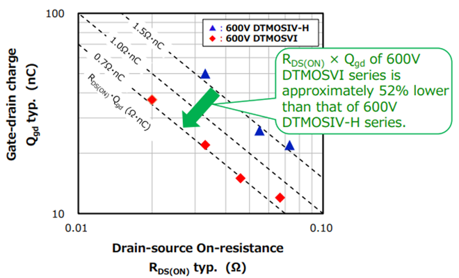
在DTMOSⅥ 600V系列(包括新产品)中,通过优化栅极设计和工艺,与具有相同额定漏源电压的东芝现有的DTMOSⅣ-H系列产品相比,漏源导通电阻和栅漏电荷的乘积(MOSFET性能的品质因数)降低了约52%。
新产品采用TO-247-4L(X)四脚封装,带有一个栅极驱动信号源端子。与TO-247三脚封装相比,TO-247-4L(X)封装支持栅极驱动信号采用开尔文接法,从而减小源极导线在封装结构内部产生的电感影响。这种方法可以增强高速开关性能,有助于提高不间断电源(UPS)、光伏逆变器等设备的高效率。
东芝还提供支持电路设计的各种工具。除了可以在短时间内验证电路功能的G0 SPICE模型外,现在还提供可以准确再现瞬态特性的高精度G2 SPICE模型。
东芝将继续扩大DTMOSⅥ 600V系列产品线,以期通过提高工业设备开关电源的效率,早日实现碳中和。
特点
- 低导通电阻RDS(ON)×Qgd(漏源导通电阻和栅漏电荷的乘积)以及开关电源(SMPS)的高效率
- 采用TO-247-4L(X)四脚封装:加装一个栅极驱动信号源极端子,以降低开关损耗。
特性说明
1.低导通电阻RDS(ON)×Qgd(漏源导通电阻和栅漏电荷的乘积)以及开关电源(SMPS)的高效率
在DTMOSⅥ 600V系列产品中,通过优化栅极设计和工艺,与具有相同额定漏源电压的东芝现有DTMOSⅣ-H系列产品相比,单位面积的漏源导通电阻值降低了约13%,栅漏电荷减小了约45%,漏源导通电阻和栅漏电荷的乘积(MOSFET性能的品质因数)降低了约52%。这意味着DTMOSⅥ系列的导通损耗与开关损耗之间的权衡关系更好,有助于提高开关电源(SMPS)的效率。
注:
[1]上述数值均由东芝测量。
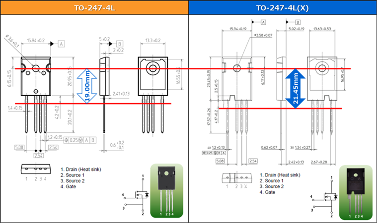
2.采用TO-247-4L(X)[2]四脚封装:加装一个栅极驱动信号源极端子,以降低开关损耗。
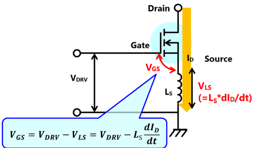
在图2所示的三脚式封装示例中,当施加栅极驱动电压VDRV时,源极导线的电感分量LS和漏极电流ID的dID/dt梯度分量会产生一个反电动势电压VLS,而产生的反电动势电压VLS会减小栅极驱动电压VDRV。因此,FET芯片的栅极与源极之间施加的电压VGS就是被反电动势电压VLS减小的栅极驱动电压VDRV。这种封装方式降低了MOSFET的开关速度。
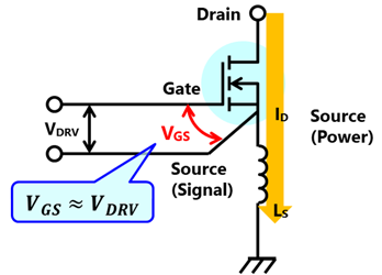
另一方面,在图3所示的四脚式封装示例中,通过连接靠近FET芯片的栅极驱动信号源极端子,可减小反电动势电压VLS的影响。因此,在四脚式封装中,栅极和源极之间施加的电压VGS与栅极驱动电压VDRV大致相同,相较于三脚式封装,这能提升MOSFET的开关速度。
注:
[2]TO-247-4L(X)封装的外观和尺寸不同于东芝现有的四脚封装TO-247-4L。请注意,在下图的箭头指示部分中,尺寸差异超过10%。如欲了解详情,敬请访问各封装的相应链接。
应用
- 开关电源(用于数据中心服务器等)
- 光电发生器的功率调节器
- 不间断电源(UPS)
主要规格
(Ta=25°C,除非另有规定)
| 器件型号 | 封装 | 绝对最大额定值 | 电气特性 | 库存查询与购买 | |||||
|---|---|---|---|---|---|---|---|---|---|
漏源电压VDSS(V) |
漏极电流(DC) ID(A) |
漏源导通电阻RDS(ON)(mΩ) |
栅极电荷总量Qg(nC) |
栅漏电荷Qgd(nC) |
输入电容Ciss(pF) |
反向恢复时间trr(ns) |
|||
| Tc=25°C | VGS=10V | VGS=10V | VGS=10V | VDS=300V | VDD=400V, -dIDR/dt =100A/μs |
||||
| 典型值 | 典型值 | 典型值 | 典型值 | 典型值 | |||||
| TK125Z60Z1 | TO-247-4L(X) | 600 | 20 | 105 | 28 | 8 | 1620 | 285 |  |
| TK099Z60Z1 | 25 | 83 | 36 | 10 | 2050 | 297 | |
||
| TK080Z60Z1 | 30 | 67 | 43 | 12 | 2510 | 345 | |
||
| TK063Z60Z1 | 37 | 53 | 56 | 15 | 3200 | 350 | |
||
| TK040Z60Z1 | 52 | 33 | 85 | 22 | 5200 | 380 | |
||
| TK024Z60Z1 | 80 | 20 | 140 | 37 | 8420 | 425 | |
||
购买、样品、及IC可靠性查询
库存查询与购买
请输入3个以上字符
Through this website you are able to proceed to the website of our distributors ("Third Party Website") which is not under the control of Toshiba Corporation and its subsidiaries and affiliates (collectively "Toshiba"). The Third Party Website is made available to you as a convenience only and you agree to use the Third Party Website at your own risk. The link of the Third Party Website does not necessarily imply a recommendation or an endorsement by Toshiba of the Third Party Website. Please be aware that Toshiba is not responsible for any transaction done through the Third Party Website, and such transactions shall be subject to terms and conditions which may be provided in the Third Party Website.
*本文提及的公司名称、产品名称和服务名称可能是其各自公司的商标。
*本文件中所含信息,包括产品价格和产品规格、服务内容及联系方式,仅于公告当日有效,如有更改,恕不另行通知。