


- 型号 & 关键词搜索
- 交叉搜索
- 参数搜索
- 库存查询与购买
This webpage doesn't work with Internet Explorer. Please use the latest version of Google Chrome, Microsoft Edge, Mozilla Firefox or Safari.
请输入3个以上字符 Search for multiple part numbers fromhere.
The information presented in this cross reference is based on TOSHIBA's selection criteria and should be treated as a suggestion only. Please carefully review the latest versions of all relevant information on the TOSHIBA products, including without limitation data sheets and validate all operating parameters of the TOSHIBA products to ensure that the suggested TOSHIBA products are truly compatible with your design and application.Please note that this cross reference is based on TOSHIBA's estimate of compatibility with other manufacturers' products, based on other manufacturers' published data, at the time the data was collected.TOSHIBA is not responsible for any incorrect or incomplete information. Information is subject to change at any time without notice.
请输入3个以上字符
N+P双通道配置的MOSFET实现了消费设备和工业设备的小型化和低功耗目标
东芝电子元件及存储装置株式会社(简称“东芝”)现已推出N+P双通道配置的30V MOSFET“SSM6L826R”。这款产品适用于消费设备和工业设备电源线的单相直流无刷电机控制、直流有刷电机控制和负载开关等应用。
新产品SSM6L826R采用了带扁平引线的TSOP6F封装(2.9×2.8×0.8mm),提高了芯片贴装能力。因此,N沟道MOSFET的漏源导通电阻(RDS(ON))低至46mΩ(最大值)(VGS=10V)[1],P沟道MOSFET的该电阻低至45mΩ(最大值)(VGS=-10V)[2],可助力实现设备的小型化和低功耗目标。
鉴于N沟道MOSFET和P沟道MOSFET的RDS(ON)数值大致相等,二者的导通损耗也几乎相同,可简化电路设计工作。此外,该产品是由N沟道MOSFET和P沟道MOSFET组成的具有独立端子的双通道配置,因此适用于驱动单相直流无刷电机和直流有刷电机。该产品也适用于负载开关应用;在这类应用场景中,P沟道MOSFET负责电源线的导通/关断开关控制,N沟道MOSFET负责控制栅极,有助于减小元器件贴片面积,减少所需的元器件数量。
这款新产品推出后,原先的双通道MOSFET(TSOP6F封装)产品线拓展至三款N+N双通道MOSFET[3]、一款P+P双通道MOSFET[3]和两款N+P双通道MOSFET[3],扩大了产品选型范围。
东芝将继续扩大消费设备和工业设备的专用MOSFET产品线,助力高效、低损耗的紧凑设计。
注:
[1]测量条件:ID=4.0A,Ta=25°C
[2]测量条件:ID=-4.0A,Ta=25°C
[3]截止2026年3月
特点
- N沟道MOSFET和P沟道MOSFET的RDS(ON)数值都很低且大致相等
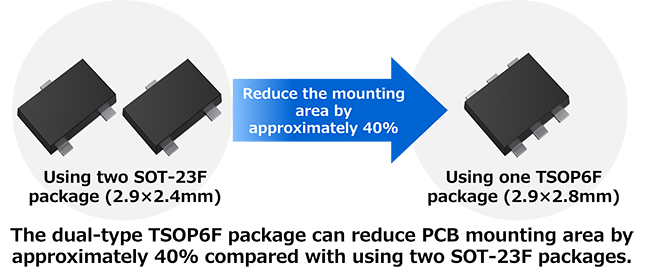
- 双通道配置(N沟道和P沟道)的MOSFET有助于减小元器件贴片面积
- 采用容许耗散功率较高的小型封装
特点说明
1.N沟道MOSFET和P沟道MOSFET的RDS(ON)数值都很低且大致相等
TN沟道MOSFET和P沟道MOSFET的RDS(ON)数值都很低且几乎相同。这种结构有助于降低设备的导通损耗和功耗。此外,由于二者的RDS(ON)数值几乎相同,因此导通损耗也几乎相同,可简化电路设计工作。
N沟道MOSFET:RDS(ON)=46mΩ(最大值)(VGS=10V)[1]
P沟道MOSFET:RDS(ON)=45mΩ(最大值)(VGS=-10V)[2]
2.双通道配置(N沟道和P沟道)的MOSFET有助于减小元器件贴片面积
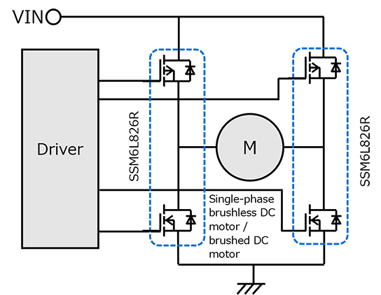
该新产品是一款N+P双通道配置的MOSFET,适用于单相直流无刷电机和直流有刷电机驱动电路,有助于减少元器件数量,减小印刷电路板(PCB)的贴片面积。
3.采用容许耗散功率功较高的小型封装
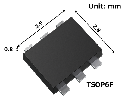
新产品采用TSOP6F小型封装(2.9×2.8×0.8mm),有助于减小贴片面积。另外,即使采用小型封装设计,扁平引线结构也能实现高达1.0W[4]的容许耗散功率(PD)。
注:
[4]测量条件:器件贴装在FR4电路板上。(总功率)(25.4×25.4×1.6mm,铜片:645mm2)
应用
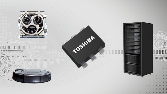
- 工业设备
服务器(冷却风扇等) - 消费设备
台式电脑(冷却风扇等)
家用电器(清洁机器人等)
医疗保健设备(电动剃须刀、电动牙刷等)
主要规格
(Ta=25°C)
| 器件型号 | 极性 | 封装 | 绝对最大额定值 | 电气特性 | 库存查询与购买 | ||||||
|---|---|---|---|---|---|---|---|---|---|---|---|
| 名称 | 尺寸(mm) | 漏-源电压VDSS (V) |
栅-源电压 VGSS (V) |
漏极电流(DC)ID (A) |
漏-源导通电阻RDS(ON)(mΩ) | 输入电容 Ciss(pF) |
栅极电荷总量(栅-源电荷加上栅-漏电荷) Qg (nC) |
||||
| VGS= |4.5V| |
VGS= |10V| |
||||||||||
| 典型值 | 最大值 | 最大值 | 典型值 | 典型值 | |||||||
| SSM6L826R | N沟道 + P沟道 |
TSOP6F | 2.9×2.8 ×0.8 |
30 | +20/-12 | 4 | 64 | 46 | 280 | 2.5 |  |
| -30 | -20/+10 | -4 | 73 | 45 | 492 | 6.2 | |||||
| SSM6L807R[5] | N沟道 + P沟道 |
TSOP6F | 2.9×2.8 ×0.8 |
30 | ±12 | 4 | 39.1 | - | 310 | 3.2 | |
| -20 | ±12 | -4 | 56 | 45 | 480 | 6.74 | |||||
| SSM6N815R[5] | N沟道(2个) | TSOP6F | 2.9×2.8 ×0.8 |
100 | ±20 | 2 | 142 | 103 | 290 | 3.1 | |
| SSM6N813R[5] | N沟道(2个) | TSOP6F | 2.9×2.8 ×0.8 |
100 | ±20 | 3.5 | 154 | 112 | 242 | 3.6 | |
| SSM6P816R[5] | P沟道(2个) | TSOP6F | 2.9×2.8 ×0.8 |
-20 | ±10 | -6 | 30.1 | - | 1030 | 16.6 | |
注:
[5]现有产品
相关内容
Selection Guide Small Signal and Logic (PDF: 8.71MB)
Introduction of small-package MOSFET (PDF: 476KB)
购买、样品、及IC可靠性查询
库存查询与购买
请输入3个以上字符
Through this website you are able to proceed to the website of our distributors ("Third Party Website") which is not under the control of Toshiba Corporation and its subsidiaries and affiliates (collectively "Toshiba"). The Third Party Website is made available to you as a convenience only and you agree to use the Third Party Website at your own risk. The link of the Third Party Website does not necessarily imply a recommendation or an endorsement by Toshiba of the Third Party Website. Please be aware that Toshiba is not responsible for any transaction done through the Third Party Website, and such transactions shall be subject to terms and conditions which may be provided in the Third Party Website.
*本文提及的公司名称、产品名称和服务名称可能是其各自公司的商标。
*本文件中所含信息,包括产品价格和产品规格、服务内容及联系方式,仅于公告当日有效,如有更改,恕不另行通知。