


- 型号 & 关键词搜索
- 交叉搜索
- 参数搜索
- 库存查询与购买
This webpage doesn't work with Internet Explorer. Please use the latest version of Google Chrome, Microsoft Edge, Mozilla Firefox or Safari.
请输入3个以上字符 Search for multiple part numbers fromhere.
The information presented in this cross reference is based on TOSHIBA's selection criteria and should be treated as a suggestion only. Please carefully review the latest versions of all relevant information on the TOSHIBA products, including without limitation data sheets and validate all operating parameters of the TOSHIBA products to ensure that the suggested TOSHIBA products are truly compatible with your design and application.Please note that this cross reference is based on TOSHIBA's estimate of compatibility with other manufacturers' products, based on other manufacturers' published data, at the time the data was collected.TOSHIBA is not responsible for any incorrect or incomplete information. Information is subject to change at any time without notice.
请输入3个以上字符
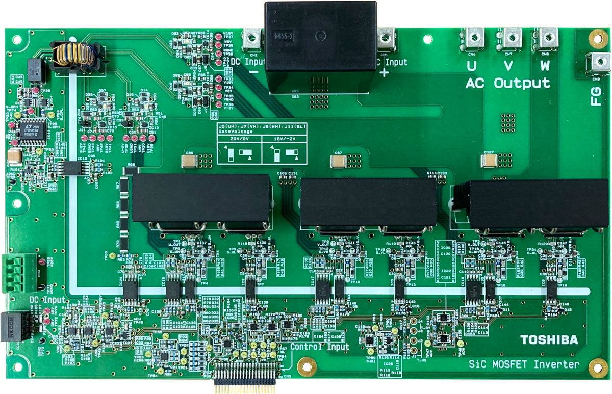
SiC MOSFET
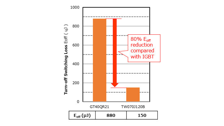
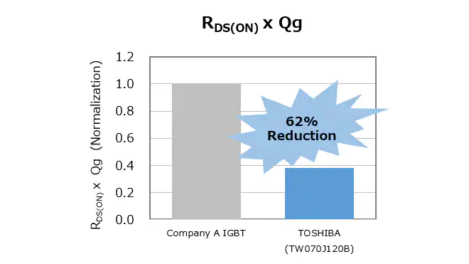
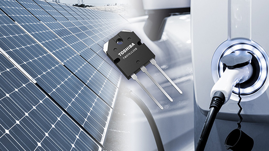
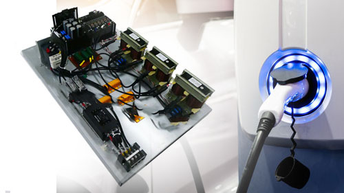
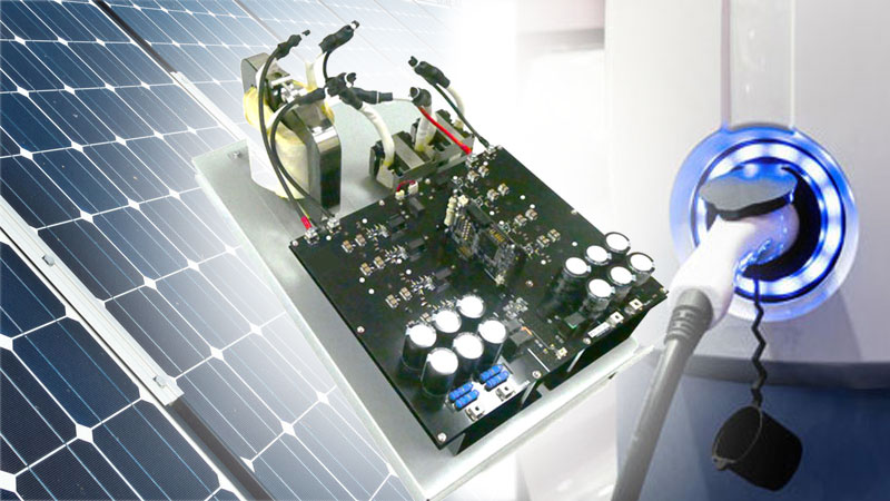
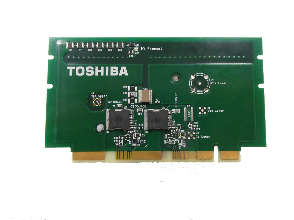
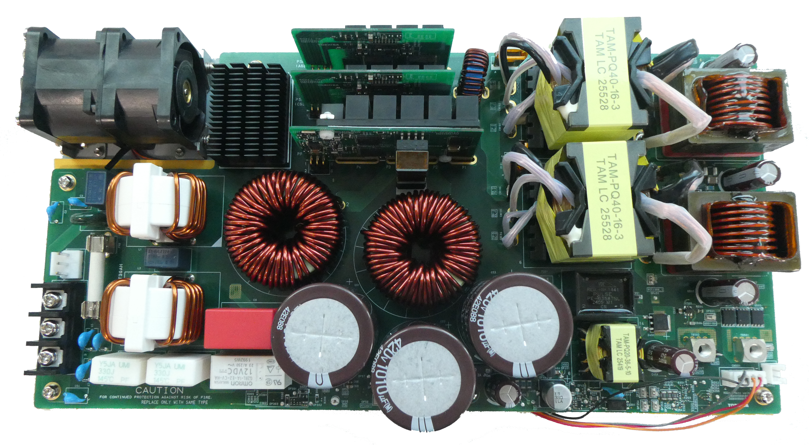
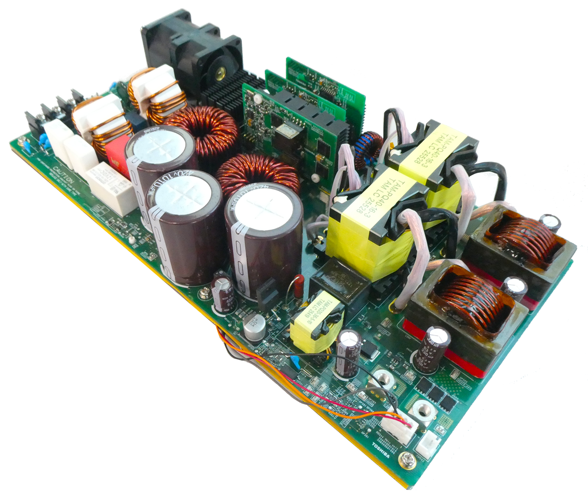
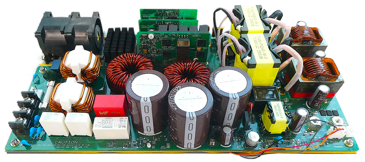
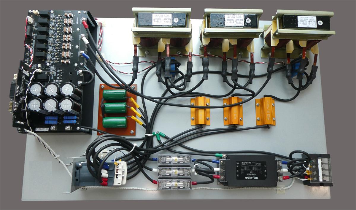
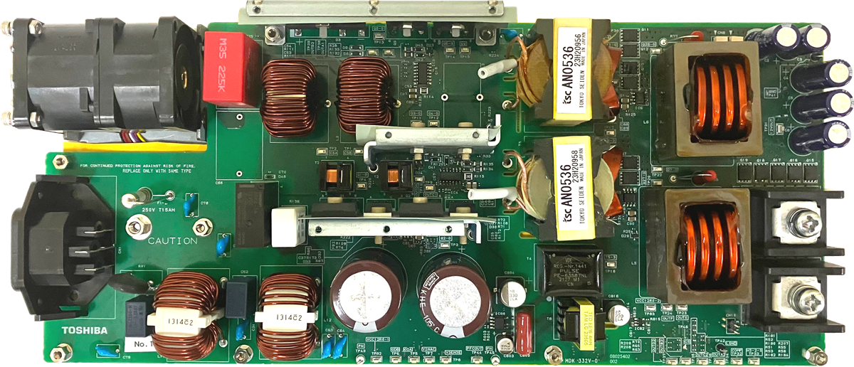
宽带隙功率半导体充分利用东芝第2代碳化硅(SiC)器件结构的优势,为高电压产品带来了极具吸引力的优势。与传统的硅(Si)功率半导体相比,东芝的SiC MOSFET具有更高的可靠性、在高温环境下的出色工作、高速开关和低导通电阻的特性。SiC MOSFET适用于大功率且高效的各类应用,包括工业电源、太阳能逆变器和UPS。
产品线
(除非另有规定,@Ta=25℃)
| 产品代 | 器件型号 | 封装 | 绝对最大额定值 | 电气特性 | 库存查询与购买 | |||||
|---|---|---|---|---|---|---|---|---|---|---|
| VDSS(V) | VGSS(V) | ID(A) | RDS(ON)(mΩ) | Vth(V) | Qg (nC) |
Ciss(pF) | ||||
| Tc=25°C | VGS=18V | VDS=10V | ||||||||
| 典型值 | 典型值 | 典型值 | ||||||||
| 第3代 | TW015N120C | TO-247 | 1200 | -10至25 | 100 | 15 | 3.0至5.0 | 158 | 6000 |  |
| TW030N120C | 60 | 30 | 82 | 2925 | |
|||||
| TW045N120C | 40 | 45 | 57 | 1969 | |
|||||
| TW060N120C | 36 | 60 | 46 | 1530 | |
|||||
| TW140N120C | 20 | 140 | 24 | 691 | |
|||||
| TW015N65C | 650 | 100 | 15 | 128 | 4850 | |
||||
| TW027N65C | 58 | 27 | 65 | 2288 | |
|||||
| TW048N65C | 40 | 48 | 41 | 1362 | |
|||||
| TW083N65C | 30 | 83 | 28 | 873 | |
|||||
| TW107N65C | 20 | 107 | 21 | 600 | |
|||||
| TW015Z120C | TO-247-4L(X) | 1200 | 100 | 15 | 158 | 6000 | |
|||
| TW030Z120C | 60 | 30 | 82 | 2925 | |
|||||
| TW045Z120C | 40 | 45 | 57 | 1969 | |
|||||
| TW060Z120C | 36 | 60 | 46 | 1530 | |
|||||
| TW140Z120C | 20 | 140 | 24 | 691 | |
|||||
| TW015Z65C | 650 | 100 | 15 | 128 | 4850 | |
||||
| TW027Z65C | 58 | 27 | 65 | 2288 | |
|||||
| TW048Z65C | 40 | 48 | 41 | 1362 | |
|||||
| TW083Z65C | 30 | 83 | 28 | 873 | |
|||||
| TW107Z65C | 20 | 107 | 21 | 600 | |
|||||
| TW031V65C | DFN 8×8 | 650 | 53 | 31 | 65 | 2288 | |
|||
| TW054V65C | 36 | 54 | 41 | 1362 | |
|||||
| TW092V65C | 27 | 92 | 28 | 873 | |
|||||
| TW123V65C | 18 | 123 | 21 | 600 | |
|||||
| TW027U65C | TOLL | 650 | 57 | 27 | 65 | 2288 | |
|||
| TW048U65C | 39 | 48 | 41 | 1362 | |
|||||
| TW083U65C | 28 | 83 | 28 | 873 | |
|||||
技术文章
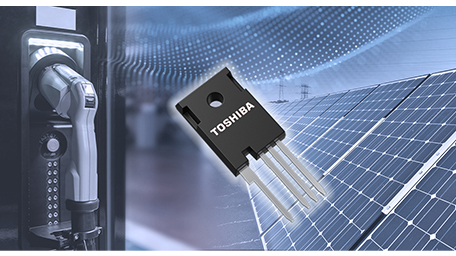
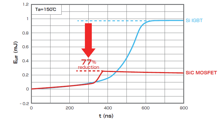
东芝第3代SiC MOSFET拥有更低的功耗,支持各种高功率密度应用,如开关电源(数据中心服务器、通信设备等)、不间断电源(UPS)、光伏逆变器、电动汽车充电站等。
文档
技术专辑
应用


参考设计
购买、样品、及IC可靠性查询
库存查询与购买
请输入3个以上字符
Through this website you are able to proceed to the website of our distributors ("Third Party Website") which is not under the control of Toshiba Corporation and its subsidiaries and affiliates (collectively "Toshiba"). The Third Party Website is made available to you as a convenience only and you agree to use the Third Party Website at your own risk. The link of the Third Party Website does not necessarily imply a recommendation or an endorsement by Toshiba of the Third Party Website. Please be aware that Toshiba is not responsible for any transaction done through the Third Party Website, and such transactions shall be subject to terms and conditions which may be provided in the Third Party Website.