


- 型号 & 关键词搜索
- 交叉搜索
- 参数搜索
- 库存查询与购买
This webpage doesn't work with Internet Explorer. Please use the latest version of Google Chrome, Microsoft Edge, Mozilla Firefox or Safari.
请输入3个以上字符 Search for multiple part numbers fromhere.
The information presented in this cross reference is based on TOSHIBA's selection criteria and should be treated as a suggestion only. Please carefully review the latest versions of all relevant information on the TOSHIBA products, including without limitation data sheets and validate all operating parameters of the TOSHIBA products to ensure that the suggested TOSHIBA products are truly compatible with your design and application.Please note that this cross reference is based on TOSHIBA's estimate of compatibility with other manufacturers' products, based on other manufacturers' published data, at the time the data was collected.TOSHIBA is not responsible for any incorrect or incomplete information. Information is subject to change at any time without notice.
请输入3个以上字符
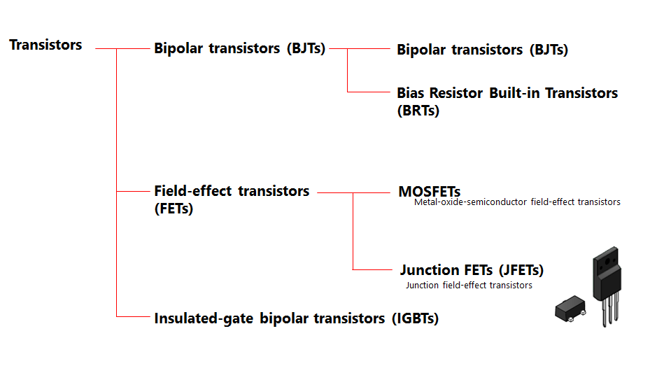
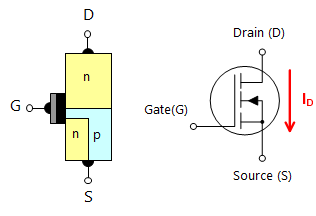
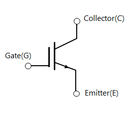
结型场效应晶体管(JFET)
下载“第Ⅲ章:晶体管” (PDF:2.0MB)
<JFET的操作>
JFET:结型场效应晶体管
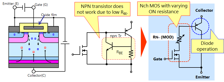
(1)在N沟道结型场效应晶体管(图3-3(a))中,当在漏极和源极之间施加电压时,电子从源极流向漏极。
(2)当在栅极和源极之间施加反向偏压时,耗尽层扩大并抑制(1)中的电子流动。(使电子流动的路径变窄)
(3)如果栅极和源极之间的反向偏压进一步增加,耗尽层就会阻塞通道,电子流动停止。
如上所示,施加在栅极和源极之间的电压控制着漏极和源极之间的状态。所以场效应晶体管是电压驱动的器件。
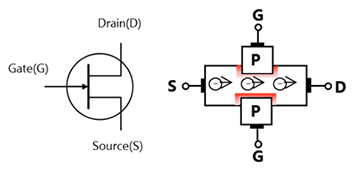
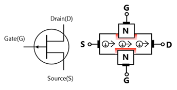
注:电流方向与电子流动方向相反。耗尽层的拓宽机理与二极管相同。
第Ⅲ章:晶体管

相关信息
- 产品
- 应用说明
- FAQ