- 型号 & 关键词搜索
- 交叉搜索
- 参数搜索
- 库存查询与购买
This webpage doesn't work with Internet Explorer. Please use the latest version of Google Chrome, Microsoft Edge, Mozilla Firefox or Safari.
请输入3个以上字符 Search for multiple part numbers fromhere.
The information presented in this cross reference is based on TOSHIBA's selection criteria and should be treated as a suggestion only. Please carefully review the latest versions of all relevant information on the TOSHIBA products, including without limitation data sheets and validate all operating parameters of the TOSHIBA products to ensure that the suggested TOSHIBA products are truly compatible with your design and application.Please note that this cross reference is based on TOSHIBA's estimate of compatibility with other manufacturers' products, based on other manufacturers' published data, at the time the data was collected.TOSHIBA is not responsible for any incorrect or incomplete information. Information is subject to change at any time without notice.
请输入3个以上字符
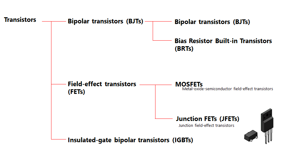
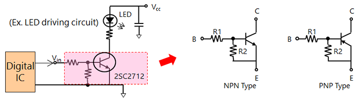
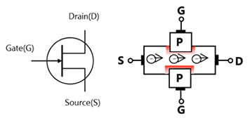
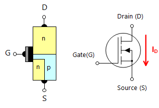
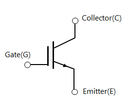
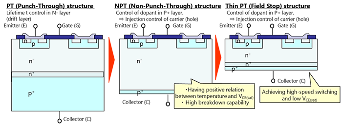
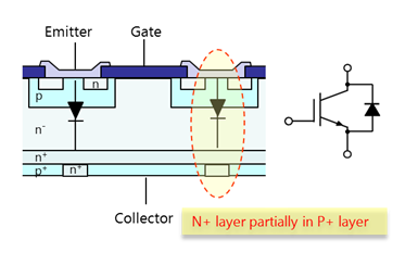
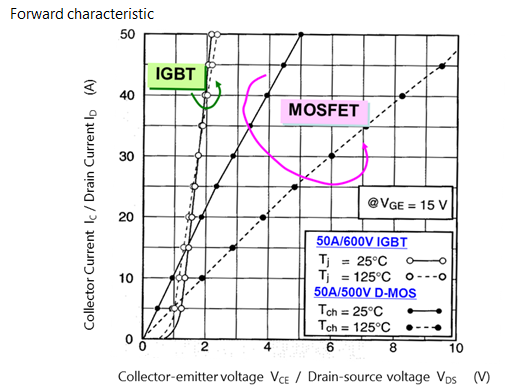
BJT和MOSFET的差异
下载“第Ⅲ章:晶体管” (PDF:2.0MB)
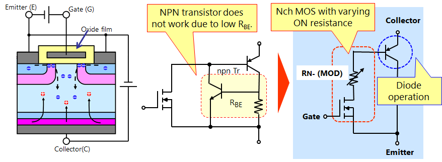
关于BJT和MOSFET开关操作差异的解释。
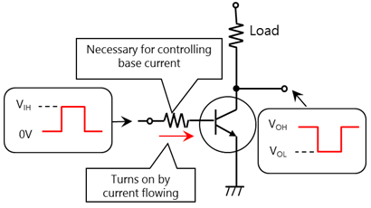
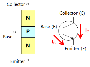
(1)基极电压升高时,BJT的基极电流开始流动,集电极电流与基极电流成正比。大约从0.7V开始发生电流流动。这个电压被称为基极-发射极阈值电压(VBE)。为了使集电极电流流动,需要提供基极电流,并且需要连续的驱动功率。(需要低驱动电压、连续驱动功率)
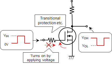
(2)由于MOSFET根据栅极-源极电压形成一个沟道,这个电压必须是一定的或更高的电压。一旦沟道形成,导通状态继续,漏极电流继续流动,因此所需的驱动功率很小。通过释放积聚在栅极中的电荷并移除沟道,它将转变为关闭状态。(驱动电压高于BJT,驱动功率小)