- 型号 & 关键词搜索
- 交叉搜索
- 参数搜索
- 库存查询与购买
This webpage doesn't work with Internet Explorer. Please use the latest version of Google Chrome, Microsoft Edge, Mozilla Firefox or Safari.
请输入3个以上字符 Search for multiple part numbers fromhere.
The information presented in this cross reference is based on TOSHIBA's selection criteria and should be treated as a suggestion only. Please carefully review the latest versions of all relevant information on the TOSHIBA products, including without limitation data sheets and validate all operating parameters of the TOSHIBA products to ensure that the suggested TOSHIBA products are truly compatible with your design and application.Please note that this cross reference is based on TOSHIBA's estimate of compatibility with other manufacturers' products, based on other manufacturers' published data, at the time the data was collected.TOSHIBA is not responsible for any incorrect or incomplete information. Information is subject to change at any time without notice.
请输入3个以上字符
降低开关噪声的对策
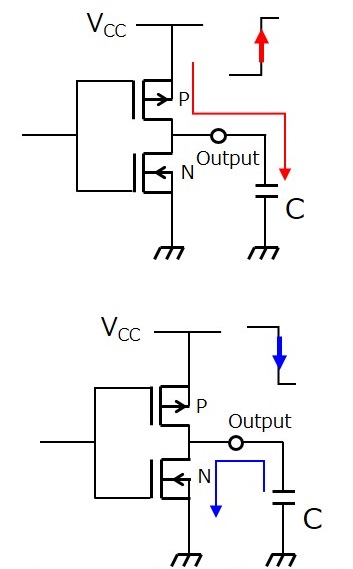
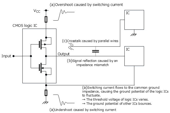
CMOS逻辑IC中的MOSFET在对内部和外部负载电容进行充放电的同时进行开关转换。开关过程中的走线阻抗可以看作是一个LCR电路。由于开关电流(i)流过电感(L),所以在CMOS逻辑IC的VCC和GND线上出现峰值电压(=L(di/dt))。这种噪声便称为开关噪声。
多个同步开关输出会消耗较大的充电/放电电流,因此会产生较大的开关噪声(称为同步开关噪声)。下面列出了降低开关噪声的措施。
降低开关噪声的对策:
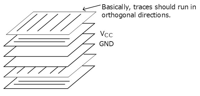
(1)分别增加和减小VCC和GND线的宽度和长度,以减小它们的电感。
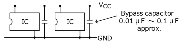
(2)将旁路电容器放置在CMOS逻辑IC的VCC和GND引脚之间并尽可能使其靠近(参见下图)。
(3)注意时钟和重置信号。未使用的门输入端(如驱动器)应连接到VCC或GND。将一个低通滤波器连接到使用的门输出端,以消除噪声。
(4)选择低噪声IC。
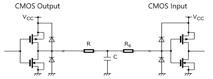
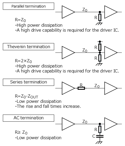
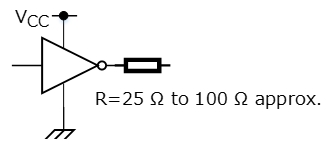
(5)在使用的门输出端添加一个阻尼电阻器(见下图)。必须检查输出波形以调整阻尼电阻器的值。

* 东芝为CMOS IC提供内部阻尼电阻器(见下图),这不仅有助于降低开关噪声,而且有助于减少零件数量。