- 型号 & 关键词搜索
- 交叉搜索
- 参数搜索
- 库存查询与购买
This webpage doesn't work with Internet Explorer. Please use the latest version of Google Chrome, Microsoft Edge, Mozilla Firefox or Safari.
请输入3个以上字符 Search for multiple part numbers fromhere.
The information presented in this cross reference is based on TOSHIBA's selection criteria and should be treated as a suggestion only. Please carefully review the latest versions of all relevant information on the TOSHIBA products, including without limitation data sheets and validate all operating parameters of the TOSHIBA products to ensure that the suggested TOSHIBA products are truly compatible with your design and application.Please note that this cross reference is based on TOSHIBA's estimate of compatibility with other manufacturers' products, based on other manufacturers' published data, at the time the data was collected.TOSHIBA is not responsible for any incorrect or incomplete information. Information is subject to change at any time without notice.
请输入3个以上字符
输入上升和下降时间规范
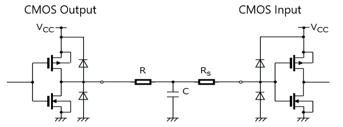
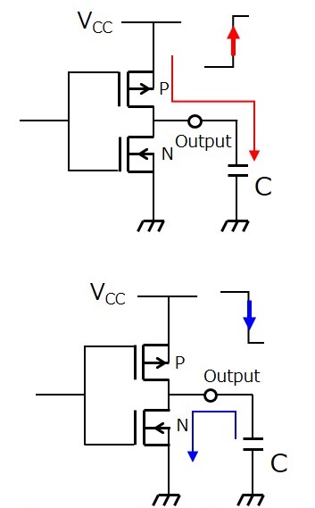
在数据表中,通用CMOS逻辑IC的输入上升和下降时间是在保证其功能运行的工作范围内规定的。
在工作范围内使用CMOS逻辑IC,防止由于输出振荡等引起的故障。
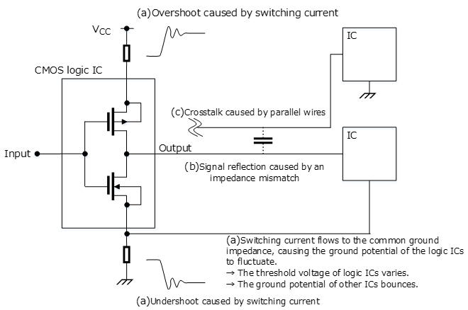
如果对输入端施加缓慢上升或下降信号(低转换速率信号),则在切换过程中会出现电流峰值,导致VCC和GND弹跳,这可能导致输出振荡或故障。
使用带有施密特触发器输入的IC来缓慢更改输入。但是如果输入变化过慢,即使带有施密特触发器输入的IC仍可能无法抑制电源或信号线上的噪声,从而导致输出振荡或不稳定。
下表显示了每个系列中典型IC*1的上升和下降时间。
| 类型 | 系列名称 | 系列型号 | 单门逻辑(L-MOS)等效 | 工作电压范围(V) | 传输延迟时间*1,tpLH和tpHL(ns) | 输出电流*2 IOUT(mA) |
3.3V时的上升和下降时间(ns/V) | 5V时的上升和下降时间(ns/V) |
|---|---|---|---|---|---|---|---|---|
适用于5V系统 |
标准型 | TC40xxB TC45xxB |
TC4S TC4W |
3至18 | 200 (当5.0V时) |
±0.51 (当5.0V时) |
0至10000ns*6 | 0至5000ns*6 |
| 高速型 | TC74HC | TC7S TC7W |
2至6 | 23 (当4.5V时) |
±4.0 or 6.0 (当4.5V时) (±2.0 in the case of TC7S) |
0至1000ns 当2V时 |
0至500ns 当4.5V时 |
|
| TC74HCT | TC7WT | 4.5至5.5 | 28 (当4.5V时) |
- | 0至500ns | |||
先进型 |
TC74AC | - | 2至5.5 | 8.5 (当4.5V时) |
±24 (当4.5V时) |
0至100ns/V | 0至20ns/V | |
| TC74ACT | - | 4.5至5.5 | 9.0 (当5.0V时) |
- | 0至10ns/V | |||
特高速型 |
TC74VHC 74VHC |
TC7SH TC7WH |
2至5.5 | 8.5 (当5.0V时) |
±8.0 (当4.5V时) |
0至100ns/V | 0至20ns/V | |
| TC74VHC9 74VHC9 |
10 (当5.0V时) |
- *5 | - *5 | |||||
| TC74VHCT 74VHCT |
TC7SET | 4.5至5.5 | 9.5 (当5.0V时) |
- | 0至20ns/V | |||
| TC74VHCV 74VHCV |
- | 1.8至5.5 | 8.5 (当5.0V时) |
±16 (当4.5V时) |
0至20ms/V | 0至1ms/V | ||
适用于低压系统 |
中速型 | TC74LCX 74LCX |
TC7SZ TC7PZ TC7WZ |
1.65至3.6 (如果是TC7SZ/PZ/WZ,则为1.65至5.5) |
6.5 (当5.0V时) |
±24 (当3.0V时) |
0至10ns/V | - |
| 高速型 | TC74VCX | 7UL | 1.2至3.6 (如果是7UL,则为0.9至3.6) |
4.2 (当2.3V时) |
±24 (当3.0V时) (如果是7UL,则为±8.0) |
0至10ns/V | - |
*1:典型IC(TC4001、TC74HC244、TC74AC244、TC74VHC244、TC74LCX244和TC74VCX244)在85°C下的最大传输延迟时间,但TC4001的最大传输延迟时间是在25°C下测得。
*2:输出电流值参见数据表中的直流特性表规定。绝对最大额定输出电流另行规定。
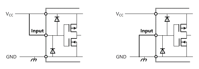
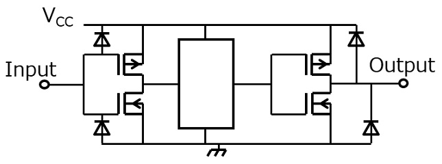
*3:TC7SET系列无输出掉电保护功能。
*4:采用fSV封装的TC7SZ系列IC无输出掉电保护功能,但具有开漏输出的IC除外。
*5:由于TC74VHC9和74VHC9系列提供施密特触发器输入,因此未指定上升和下降时间。
*6:数据表中未规定上升和下降时间。上述值仅作为设计指导。