- 型号 & 关键词搜索
- 交叉搜索
- 参数搜索
- 库存查询与购买
This webpage doesn't work with Internet Explorer. Please use the latest version of Google Chrome, Microsoft Edge, Mozilla Firefox or Safari.
请输入3个以上字符 Search for multiple part numbers fromhere.
The information presented in this cross reference is based on TOSHIBA's selection criteria and should be treated as a suggestion only. Please carefully review the latest versions of all relevant information on the TOSHIBA products, including without limitation data sheets and validate all operating parameters of the TOSHIBA products to ensure that the suggested TOSHIBA products are truly compatible with your design and application.Please note that this cross reference is based on TOSHIBA's estimate of compatibility with other manufacturers' products, based on other manufacturers' published data, at the time the data was collected.TOSHIBA is not responsible for any incorrect or incomplete information. Information is subject to change at any time without notice.
请输入3个以上字符
ESD防护的对策
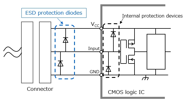
CMOS逻辑IC提供符合国际标准的静电放电(ESD)抗扰度。接触较高的静电放电可能会导致CMOS逻辑IC故障或永久性损坏。
因为CMOS逻辑IC输入门的氧化膜非常薄(几百至几千埃),所以它可能会被几百到几千伏特的ESD损坏。
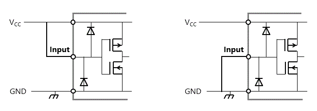
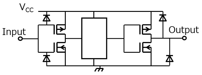
为防止这种情况,每个输入引脚通常提供ESD保护电路。但这种保护有限。对可能接触过度ESD的输入端插入外部ESD保护二极管(例如,连接到电路板外部接口的输入端)。

我们提供多种ESD模型。下面介绍一种主要的ESD模型。
人体模型(HBM)
该模型的特点是易受人体可能产生的ESD损害的影响。
关于人体电容有许多讨论。对于静电放电抗扰度测试,将使用一个100pF电容器和一个1500Ω放电电阻器模拟带电人体。在测试过程中,电容器充满电,然后通过电阻器放电。
HBM测试电路如下所示。
- 上一篇
- 16/16


