- 型号 & 关键词搜索
- 交叉搜索
- 参数搜索
- 库存查询与购买
This webpage doesn't work with Internet Explorer. Please use the latest version of Google Chrome, Microsoft Edge, Mozilla Firefox or Safari.
请输入3个以上字符 Search for multiple part numbers fromhere.
The information presented in this cross reference is based on TOSHIBA's selection criteria and should be treated as a suggestion only. Please carefully review the latest versions of all relevant information on the TOSHIBA products, including without limitation data sheets and validate all operating parameters of the TOSHIBA products to ensure that the suggested TOSHIBA products are truly compatible with your design and application.Please note that this cross reference is based on TOSHIBA's estimate of compatibility with other manufacturers' products, based on other manufacturers' published data, at the time the data was collected.TOSHIBA is not responsible for any incorrect or incomplete information. Information is subject to change at any time without notice.
请输入3个以上字符
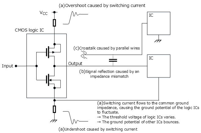
信号反射的对策
对于高速CMOS逻辑IC,反射会导致信号延迟、振铃、过冲和欠冲增加。
传输线路反射:典型走线的特性阻抗(*1)为50至150Ω。但是高速CMOS逻辑IC的I/O阻抗与典型走线的特性阻抗不同。这种阻抗的不匹配将导致一部分发射信号被反射到传输线路的发送端和接收端。
信号反射不影响缓慢上升的输出,因其上升周期与反射信号的上升周期重叠。
当反射信号上升后返回到输出时,即当下列等式成立时,信号反射才会导致问题:
tr < 2T
tr:输出信号上升时间
T:从传输线路的发送端到接收端的传输延迟时间
假设输出上升时间为3ns,沿传输线路的传输延迟时间为5ns/m。
当传输线路为30cm或更长时,信号反射会产生显著影响。
*1特性阻抗
特性阻抗是传输线路(如电路板迹线、同轴电缆)的特性之一。
传输线路特性阻抗的一般表达式是Z_0=√(L/C),其中L是单位长度的电感,C是单位长度的电容。特性阻抗的单位为欧姆(Ω)。当50Ω的终端电阻器连接到特性阻抗为50Ω的传输线路末端时,连接点处不会发生信号反射。
如果特性阻抗与电阻值不匹配,则在连接点处会发生信号反射。
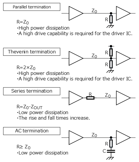
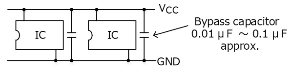
减少信号反射的对策
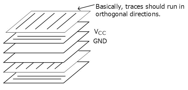
(1)提高电路板组装密度,减少电路板走线的长度,以减小其电感和电容。但是在这种情况下,需要注意相邻轨迹之间的串扰。(有关串扰,见下页。)
(2)不要使用输出电流高于必要值的IC。
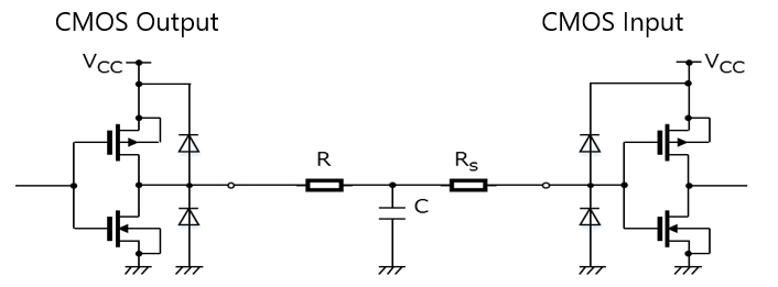
(3)提供电气终端,以便CMOS逻辑IC的I/O阻抗与传输线路的特性阻抗匹配(见下图)。
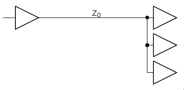
(4)当一个CMOS逻辑IC的输出驱动多个CMOS逻辑IC时,输出走线应在靠近被驱动IC的位置呈扇形展开。