- 型号 & 关键词搜索
- 交叉搜索
- 参数搜索
- 库存查询与购买
This webpage doesn't work with Internet Explorer. Please use the latest version of Google Chrome, Microsoft Edge, Mozilla Firefox or Safari.
请输入3个以上字符 Search for multiple part numbers fromhere.
The information presented in this cross reference is based on TOSHIBA's selection criteria and should be treated as a suggestion only. Please carefully review the latest versions of all relevant information on the TOSHIBA products, including without limitation data sheets and validate all operating parameters of the TOSHIBA products to ensure that the suggested TOSHIBA products are truly compatible with your design and application.Please note that this cross reference is based on TOSHIBA's estimate of compatibility with other manufacturers' products, based on other manufacturers' published data, at the time the data was collected.TOSHIBA is not responsible for any incorrect or incomplete information. Information is subject to change at any time without notice.
请输入3个以上字符
pn结
下载“第Ⅰ章:半导体基础” (PDF:1.2MB)
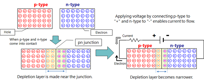
The interface between a p-type semiconductor and an n-type semiconductor is called a pn junction. When a p-type semiconductor and an n-type semiconductor are joined (not actually joined, but formed by doping so that they are adjacent to each other), the carriers, holes and free electrons, are attracted to each other and combine and disappear near the boundary. Since there are no carriers in this area, it is called a depletion layer and is in the same state as an insulator. (No bias state)
- Forward direction (connect the positive pole to the p-type region and the negative pole to the n-type region and apply voltage):
When the applied voltage is gradually increased and exceeds the forward voltage (about 0.7V for Si), electrons flow one after another from the n-type region to the p-type region, and electrons that do not combine with holes and disappear move to the positive pole, allowing current to flow. For an explanation of the physical properties of a pn junction, see the following e-learning.
Basics of Schottky Barrier Diodes 1-3. pn junction
- Reverse direction (connect the negative pole to the p-type region and the positive pole to the n-type region and apply voltage):
No current flows. In the normal voltage range, the excess electrons in the n-type semiconductor move away from the boundary surface. The holes in the p-type semiconductor also move away from the boundary surface. This causes the depletion layer near the boundary surface to expand. However, if a voltage exceeding the breakdown voltage is applied, the pn junction enters a breakdown state due to the Zener effect (avalanche effect) and current flows suddenly. In a typical diode, this breakdown causes the performance to deteriorate and be destroyed.