- 型号 & 关键词搜索
- 交叉搜索
- 参数搜索
- 库存查询与购买
This webpage doesn't work with Internet Explorer. Please use the latest version of Google Chrome, Microsoft Edge, Mozilla Firefox or Safari.
请输入3个以上字符 Search for multiple part numbers fromhere.
The information presented in this cross reference is based on TOSHIBA's selection criteria and should be treated as a suggestion only. Please carefully review the latest versions of all relevant information on the TOSHIBA products, including without limitation data sheets and validate all operating parameters of the TOSHIBA products to ensure that the suggested TOSHIBA products are truly compatible with your design and application.Please note that this cross reference is based on TOSHIBA's estimate of compatibility with other manufacturers' products, based on other manufacturers' published data, at the time the data was collected.TOSHIBA is not responsible for any incorrect or incomplete information. Information is subject to change at any time without notice.
请输入3个以上字符
p型半导体
下载“第Ⅰ章:半导体基础” (PDF:1.2MB)
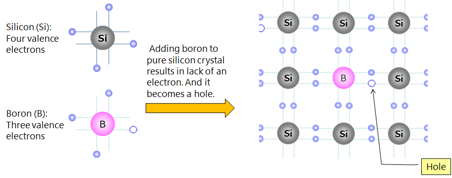
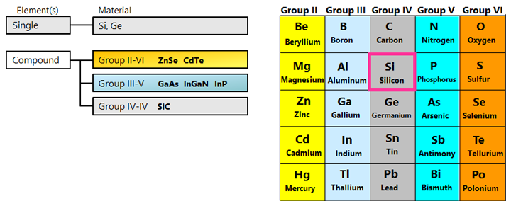
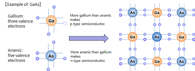
A p-type semiconductor is a group IV intrinsic semiconductor such as silicon (Si) doped with group III boron (B) or indium (In) as an impurity.
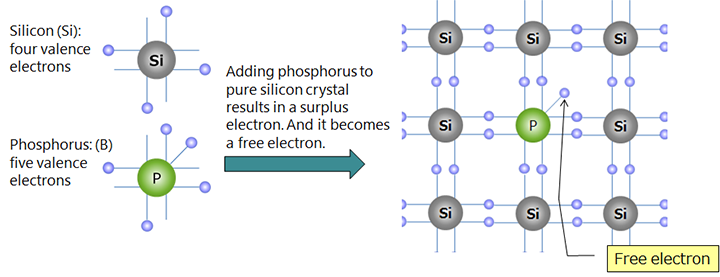
Group IV elements are tetravalent elements with four valence electrons, while group III elements are trivalent elements with three valence electrons. A single crystal made only of tetravalent elements such as Si is an intrinsic semiconductor in which all bonds are connected to other elements by covalent bonds. When a small amount of boron is added to this single crystal (diffusion/doping), an electron becomes insufficient at one of the bonds between silicon and boron, creating a hole where an electron is missing. This hole is called a hole. When a voltage is applied in this state, a nearby electron moves to the hole, so the place where the electron was becomes a new hole, and it appears that the holes move one after another to the negative pole.
In a p-type semiconductor, the particles (carriers) that carry the charge are holes. Since holes are the parts where there is a shortage of electrons, they have a positive charge. For this reason, they are called p-type.
*这个空穴就是p型半导体的载流子。

