- 型号 & 关键词搜索
- 交叉搜索
- 参数搜索
- 库存查询与购买
This webpage doesn't work with Internet Explorer. Please use the latest version of Google Chrome, Microsoft Edge, Mozilla Firefox or Safari.
请输入3个以上字符 Search for multiple part numbers fromhere.
The information presented in this cross reference is based on TOSHIBA's selection criteria and should be treated as a suggestion only. Please carefully review the latest versions of all relevant information on the TOSHIBA products, including without limitation data sheets and validate all operating parameters of the TOSHIBA products to ensure that the suggested TOSHIBA products are truly compatible with your design and application.Please note that this cross reference is based on TOSHIBA's estimate of compatibility with other manufacturers' products, based on other manufacturers' published data, at the time the data was collected.TOSHIBA is not responsible for any incorrect or incomplete information. Information is subject to change at any time without notice.
请输入3个以上字符
什么是半导体?
下载“第I章:半导体基础” (PDF:1.2MB)
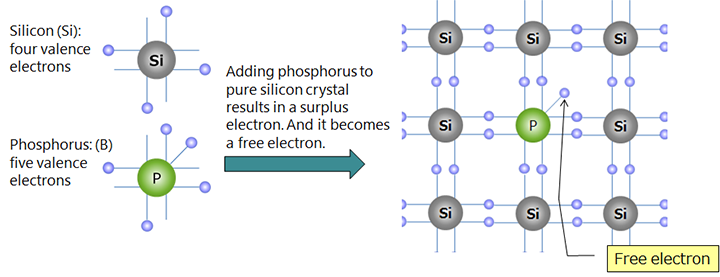
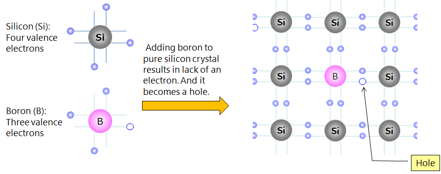
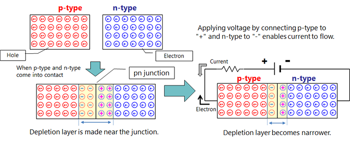
"半导体" 是一种介于导电性良好的“导体”(如金属)和几乎不导电的“绝缘体”之间的材料。 通过向不含杂质的本征半导体中添加杂质(扩散/掺杂),可以产生N型和P型两种半导体。当施加电压、电流、光、热等时,它们将表现出导体或绝缘体的特性。此外,通过将这些器件组合在一起,还可以制造出二极管、晶体管和集成电路(IC)等设备。
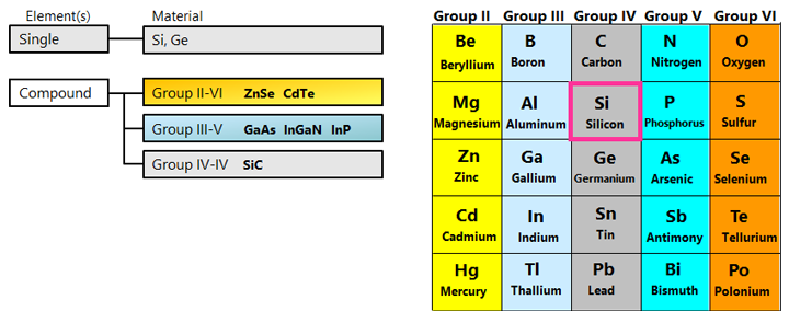
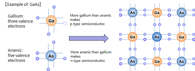
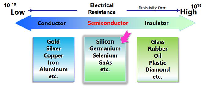
电流流动的难易程度与材料的电阻大小有关。电阻大,电流不易通过;电阻小,电流容易通过。当用电阻率来表示电流通过的难易程度时,导体为:10-8至10-4 Ωcm,绝缘体为:108至1018 Ωcm,而半导体的范围约为10-4至108 Ωcm。导体包括金、银、铜、铁和铝。绝缘体包括玻璃、橡胶、油和塑料。半导体包括硅(Si)和锗(Ge)等单一元素,以及砷化镓(GaAs)、碳化硅(SiC)、硅锗(SiGe)和氮化镓(GaN)等化合物。
- 1/7
- 下一篇