- 型号 & 关键词搜索
- 交叉搜索
- 参数搜索
- 库存查询与购买
This webpage doesn't work with Internet Explorer. Please use the latest version of Google Chrome, Microsoft Edge, Mozilla Firefox or Safari.
请输入3个以上字符 Search for multiple part numbers fromhere.
The information presented in this cross reference is based on TOSHIBA's selection criteria and should be treated as a suggestion only. Please carefully review the latest versions of all relevant information on the TOSHIBA products, including without limitation data sheets and validate all operating parameters of the TOSHIBA products to ensure that the suggested TOSHIBA products are truly compatible with your design and application.Please note that this cross reference is based on TOSHIBA's estimate of compatibility with other manufacturers' products, based on other manufacturers' published data, at the time the data was collected.TOSHIBA is not responsible for any incorrect or incomplete information. Information is subject to change at any time without notice.
请输入3个以上字符
线性稳压器的工作原理
下载“第Ⅳ章:本地电源IC” (PDF:770KB)
串联稳压器
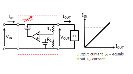
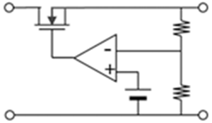
如左下图所示,不需要外部组件。(需要输入/输出电容器)
MOSFET作为可变电阻进行工作,因此输出电压变为恒定电压。
MOSFET的漏极和源极之间的电位差(VIN-VOUT)×输入电流(IIN)将产生损耗。例如,如果输入是5V,输出是3V,则效率是60%。它用于要求低噪声和精确输出电压的电路电源。
并联稳压器
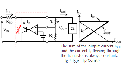
右下图中虚线所包围的区域是IC。它需要三个外部电阻。内置晶体管作为可变电阻进行工作,因此IK+IOUT=IIN=常数。其结果是,在RSD处产生的电压变为恒定,并且输出电压变为恒定电压。但除了输出电流外,还需要通过晶体管的阴极电流。此外,在输入侧电阻RSD处存在电压降,这将降低效率。它用于低电流(~20mA)应用,比如开关电源参考电压和开关电源光耦驱动电路。
