
DCA121102

新产品

Isolation Amplifiers(Digital Isolators)

产品概要

Number of Circuits 2
Function Isolation Amplifier
Application Scope Motor Phase Current and voltage Sensing / Inverter Current and voltage Sensing
Feature Sigma-delta(Σ-Δ)analog-to-digital converter technology / Magnetic coupled isolation amplifier(Digital Isolators)
Output Interface Analog output
Overcurrent high-speed feedback (Option) Available
RoHS Compatible Product (s) (#) Available

封装

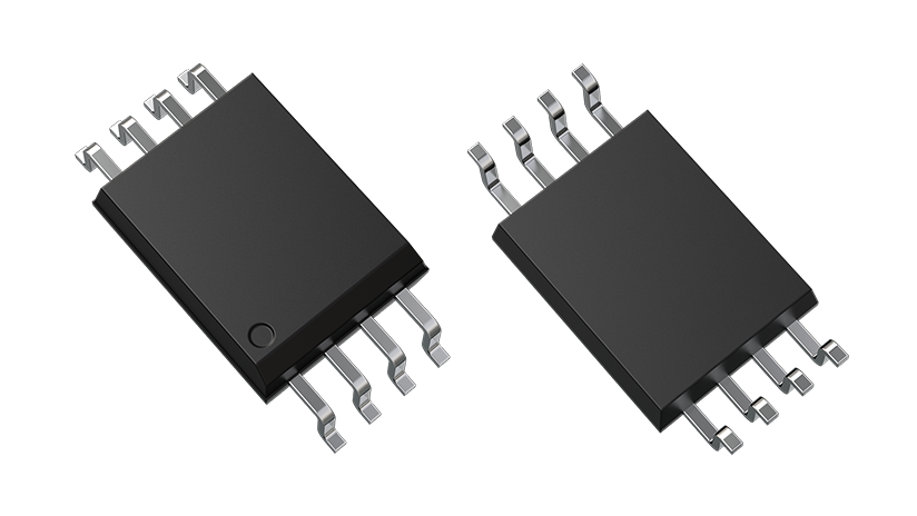
Toshiba Package Name SOIC8-W(P-SOP8-0806-1.27-001)
Package Image 东芝 DCA121102 Isolation Amplifiers(Digital Isolators)产品 SOIC8-W(P-SOP8-0806-1.27-001) 封装图片
Pins 8
Mounting Surface Mount
Width×Length×Height
(mm)
5.85×11.5×2.79
Package Dimensions 查看
SamacSys CAD model
(Symbol, Footprint and 3D model)
Download from SamacSys<br>*1 *2

Download from SamacSys
*1 *2

 Please refer to the link destination to check the detailed size.

*1

SamacSys is a wholly owned subsidiary of Supplyframe, Inc. CAD models (Symbol/Footprint /3D model) are provided by Supplyframe, Inc. The footprints are generated based on the specifications of SamacSys.

*2

Please note that the footprint dimensions may differ from the reference Land Pattern dimensions provided on our website.

绝对最大额定值

项目 符号 值 单位
Supply Voltage VDD1 VDD1 -0.5 to 6 V
Supply Voltage VDD2 VDD2 -0.5 to 6 V
Operating Temperature Topr -40 to 125 ℃

电气特性

项目 符号 条件 值 单位
Input side supply voltage VDD1 - 3.0 to 5.5 V
Output side supply voltage VDD2 - 3.0 to 5.5 V
Isolation voltage BVs
@1minute (Min)
BVS t=60sec 5000 Vrms
Input Voltage (Linear Region) (Max) VIN+, VIN- - 250 mV
Input Voltage (Linear Region) (Min) VIN+, VIN- - -250 mV
Input offset voltage (Max) VOS Ta=25℃ 0.20 mV
Input offset voltage (Min) VOS Ta=25℃ -3.0 mV
Input offset voltage (Typ.) VOS Ta=25℃ -0.05 mV
Input offset voltage drift vs ambient temperature (Max) |dVOS/dTa| - 2 μV/℃
Input offset voltage drift vs ambient temperature (Typ.) |dVOS/dTa| - 0.3 μV/℃
VOUT nonlinearity (Max) NL Ta>=-40℃
Ta<=125℃
VIN+>=-250mV
VIN+<=250mV
0.02 %
VOUT nonlinearity (Min) NL Ta>=-40℃
Ta<=125℃
VIN+>=-250mV
VIN+<=250mV
-0.02 %
Propagation delay time (50% - 50%) (Max) tpD50 CL=15pF
VIN+>=-250mV
VIN+<=250mV
1.95 μs
Propagation delay time (50% - 50%) (Typ.) tpD50 CL=15pF
VIN+>=-250mV
VIN+<=250mV
1.60 μs
common mode transient immunity (Min) CMTI - 100 kV/μs
Signal-to-noise ratio (Min) SNR - 80 dB
Signal-to-noise ratio (Typ.) SNR - 85 dB
购买及样品申请
请联系东芝官方代理商或就近联系我们的销售网点。
您可以通过以下链接搜索及购买少量样品。

文档

  • 如果该复选框不能被选中,则不能批量下载相应的文档。

Nov,2026

Nov,2026

Nov,2026

可订购器件型号

Orderable part number
(example)
MOQ(pcs) Reliability
Information
RoHS 库存查询
DCA121102(T,E 1000 Yes

技术咨询

联系我们

联系我们

常见问题

常见问题(FAQ)

Notes

返回列表页
Membership registration required
在新窗口打开