- 型号 & 关键词搜索
- 交叉搜索
- 参数搜索
- 库存查询与购买
This webpage doesn't work with Internet Explorer. Please use the latest version of Google Chrome, Microsoft Edge, Mozilla Firefox or Safari.
请输入3个以上字符 Search for multiple part numbers fromhere.
The information presented in this cross reference is based on TOSHIBA's selection criteria and should be treated as a suggestion only. Please carefully review the latest versions of all relevant information on the TOSHIBA products, including without limitation data sheets and validate all operating parameters of the TOSHIBA products to ensure that the suggested TOSHIBA products are truly compatible with your design and application.Please note that this cross reference is based on TOSHIBA's estimate of compatibility with other manufacturers' products, based on other manufacturers' published data, at the time the data was collected.TOSHIBA is not responsible for any incorrect or incomplete information. Information is subject to change at any time without notice.
请输入3个以上字符
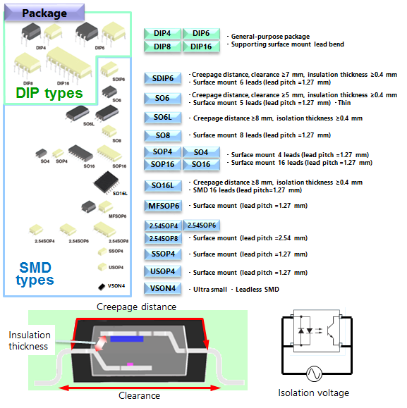
光耦的类型(封装)
下载“第Ⅴ章:光半导体” (PDF:1.8MB)
光耦必须具有符合安全标准的封装形状和介电强度。根据安全标准进行设计时,需要检查以下各项。
绝缘爬电距离
两个导体之间沿绝缘体表面的最短距离(原边和副边)。
间隙
通过空气测量的两个导体之间的最短距离。
绝缘厚度
两个导体之间绝缘体的最小距离。
隔离电压
两个导体之间的隔离电压 *
根据UL规定,即使施加1分钟也不会破坏绝缘的交流电压。
*隔离电压在2500Vrms至5000Vrms之间的产品是主流产品。
