- 型号 & 关键词搜索
- 交叉搜索
- 参数搜索
- 库存查询与购买
This webpage doesn't work with Internet Explorer. Please use the latest version of Google Chrome, Microsoft Edge, Mozilla Firefox or Safari.
请输入3个以上字符 Search for multiple part numbers fromhere.
The information presented in this cross reference is based on TOSHIBA's selection criteria and should be treated as a suggestion only. Please carefully review the latest versions of all relevant information on the TOSHIBA products, including without limitation data sheets and validate all operating parameters of the TOSHIBA products to ensure that the suggested TOSHIBA products are truly compatible with your design and application.Please note that this cross reference is based on TOSHIBA's estimate of compatibility with other manufacturers' products, based on other manufacturers' published data, at the time the data was collected.TOSHIBA is not responsible for any incorrect or incomplete information. Information is subject to change at any time without notice.
请输入3个以上字符
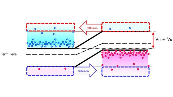
1-3-2.反向偏置

VR的反向偏置会导致扩散电位因VR而增加。虽然电子是n型半导体中的多数载流子和p型半导体中的少数载流子,但p型半导体的电子密度变得高于扩散势垒上方的n型半导体,即VD + VR(相对于无偏置和正向偏置的状态)。因此,作为p型半导体中的少数载流子的电子扩散至n型半导体中。反向偏置下发生的少数载流子扩散量远远小于正向偏置下发生的少数载流子扩散量。然而,在反向偏置下,电子被注入到p型半导体中以补偿扩散,而空穴被注入(即,电子被抽离)n型半导体。因此,反向偏置下电流的流动方向与正向偏置下的方向相反。由于少数载流子扩散,反向电流非常低。
- Prev
- 6/6

