
- General Top View
-
SEMICONDUCTOR View
-
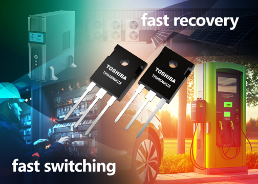
Applications
Body Electronics
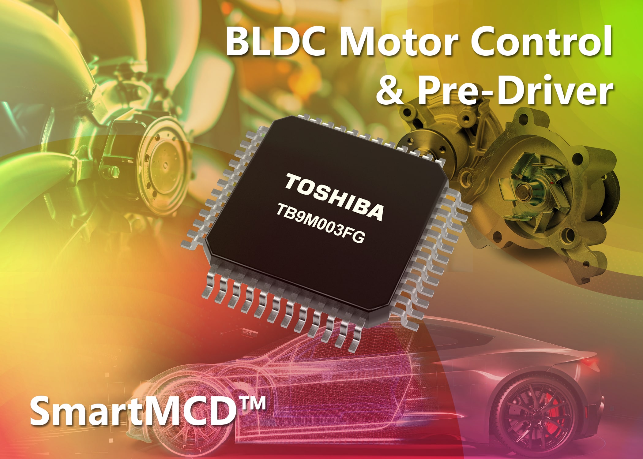
xEV
In-Vehicle Infotainment
Advanced Driver-Assistance Systems (ADAS)
Chassis
Infrastructure
BEMS/HEMS
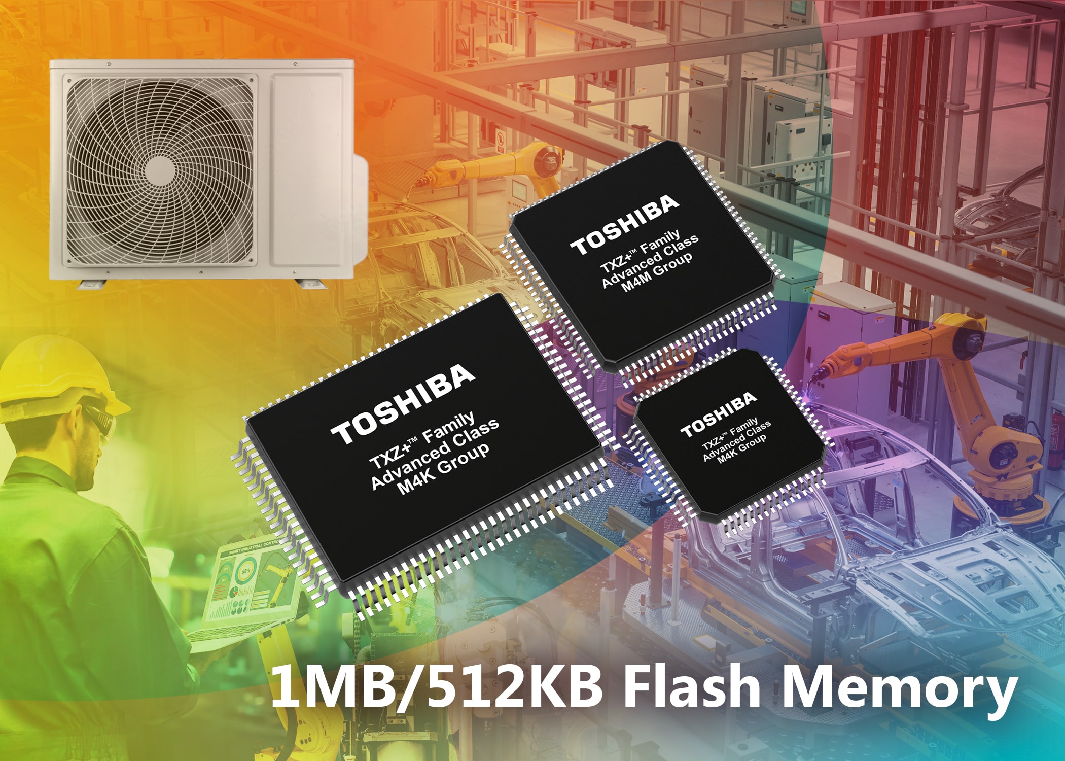
Factory Automation
Commercial Equipment
IoT Equipment
Healthcare
Wearable Device
Mobile
Computer Peripherals
-
Products
Products
-
Design & Development
Design & Development
Innovation Centre
At the Toshiba Innovation Centre we constantly strive to inspire you with our technologies and solutions. Discover how to place us at the heart of your innovations.
-
Knowledge
Knowledge
Highlighted Topics
Further Materials
Other
- Where To Buy View
-
- STORAGE View
- COMPANY View


- Part Number Search
- Cross Reference Search
- Keyword Search
- Parametric Search
- Stock Check & Purchase
This webpage doesn't work with Internet Explorer. Please use the latest version of Google Chrome, Microsoft Edge, Mozilla Firefox or Safari.
require 3 characters or more.
The information presented in this cross reference is based on TOSHIBA's selection criteria and should be treated as a suggestion only. Please carefully review the latest versions of all relevant information on the TOSHIBA products, including without limitation data sheets and validate all operating parameters of the TOSHIBA products to ensure that the suggested TOSHIBA products are truly compatible with your design and application.
Please note that this cross reference is based on TOSHIBA's estimate of compatibility with other manufacturers' products, based on other manufacturers' published data, at the time the data was collected.
TOSHIBA is not responsible for any incorrect or incomplete information. Information is subject to change at any time without notice.
require 3 characters or more.
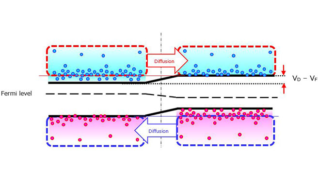
1-3-2. Reverse biasing
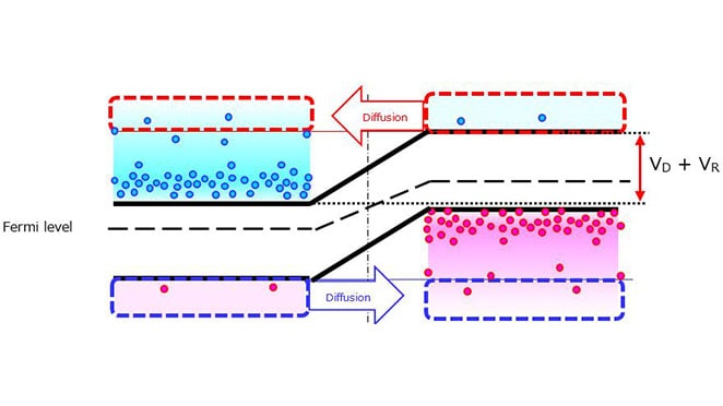
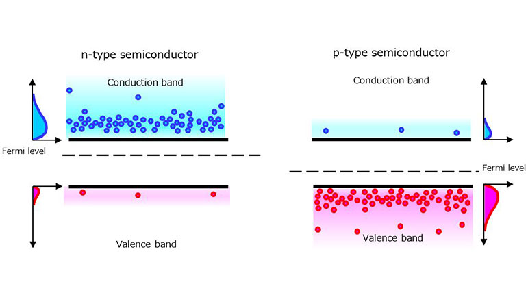
A reverse bias of VR causes the diffusion potential to increase by VR. Although electrons are the majority carriers in the n-type semiconductor and the minority carriers in the p-type semiconductor, the electron density of the p-type semiconductor becomes higher than that of the n-type semiconductor above the diffusion barrier, VD + VR (as opposed to the unbiased and forward-biased states). As a result, electrons, the minority carriers in the p-type semiconductor, diffuse into the n-type semiconductor. The amount of minority carrier diffusion that occurs under reverse bias is much smaller than that that occurs under forward bias. However, under reverse bias, electrons are injected into the p-type semiconductor to compensate for the diffusion while holes are injected into (i.e., electrons are drawn away from) the n-type semiconductor. Therefore, under reverse bias, current flows in the direction opposite to the one under forward bias. The reverse current is very low as it is due to minority carrier diffusion.
- Prev
- 6/6
Related information
- Products
Schottky Barrier Diodes - Applidcation Notes
Application Notes - FAQs
Diodes - Parametric Search
Schottky Barrier Diodes - Stock Check & Purchase
Stock Check & Purchase