适用于工业设备的MOSFET和IGBT栅极驱动电路的光耦

Photocoupler for MOSFET and IGBT Gate Driver Suitable for Industrial Equipment

Toshiba Electronic Devices & Storage Corporation ("Toshiba") has launched a new photocoupler, “TLP5795H,” and expanded its lineup to control 1A to 5A class gate drive currents for small to medium-capacity MOSFET and IGBT gate drives. Shipments start today.

In recent years, with the expansion of the green energy and factory automation markets, the demand for isolated gate drivers that drive from low-voltage control side to high-voltage power devices through isolation has been increasing. In these markets, the demand for specifications that more accurately capture the driving performance of isolated gate drivers has also been increasing. In response, Toshiba has released the TLP5795H, which specifies output current characteristics IOLH and IOHL as typical values of -4.5/+5.3A (typ.). Furthermore, Toshiba is also developing[1] the TLP5794H with -6.0/+4.0A (typ.) and the TLP5791H with -1.0/+1.0A (typ.).

The TLP5795H has a performance of -4.5/+5.3A for peak high-level/low-level output current (IOLH/IOHL), with a UVLO[2] threshold voltage (VUVLO+) of 13.5V (max), a UVLO threshold voltage (VUVLO-) of 11.1V (min), and UVLO hysteresis (UVLOHYS) of 1.0V (typ.). These values are designed to drive SiC MOSFETs with a wide gate negative bias voltage rating, as well as IGBTs. It is suitable for driving power devices with a positive bias of 15 to 20V and a negative bias of approximately 0 to -10V. For details, please refer to the application note "Gate Drive Coupler Notes on using power device gate negative bias power supply". The propagation delay time has low temperature dependence, allowing for stable operation within the practical range defined by FA equipment.

Additionally, the TLP5795H is a rail to rail[3] output device that enables switching characteristics with less voltage drop from the power supply voltage.

Furthermore, by improving the light output of the input-side infrared light-emitting diode and optimizing the design of the light-receiving element (photodiode array), Toshiba has enhanced the optical coupling efficiency and achieved an operating temperature rating of -40°C to 125°C. This allows for use in industrial equipment operating in severe thermal environments, such as PV inverters, UPS[4], and EV stands. Propagation delay time and propagation delay skew are also standardized within the operating temperature rating range.

TLP5795H is housed in a small SO6L package and contributes to improved flexibility in component placement on the set board. In addition, the new product features a minimum creepage distance of 8.0mm and an isolation voltage of 5000Vrms, allowing it to be used in equipment that requires high isolation performance.

Toshiba will continue to develop and expand its lineup of photocouplers for MOSFET and IGBT gate drive applications in industrial equipment.

Figure 1.Example of IGBT gate drive application circuit

Notes:
[1] TLP5794H and TLP5791H are scheduled for released in June 2025.
[2] UVLO: Under Voltage Lock Out. It means the function to prevent malfunction at low voltage.
[3] Rail to rail: It refers to the ability of the output voltage to cover the entire range of the power supply voltage (from the positive power rail to the negative power rail). Useful in applications that require circuits to operate at low voltages or to process signals across the entire range of supply voltages.
[4] UPS: Uninterruptible Power Supply

适用于工业设备的MOSFET和IGBT栅极驱动电路的光耦

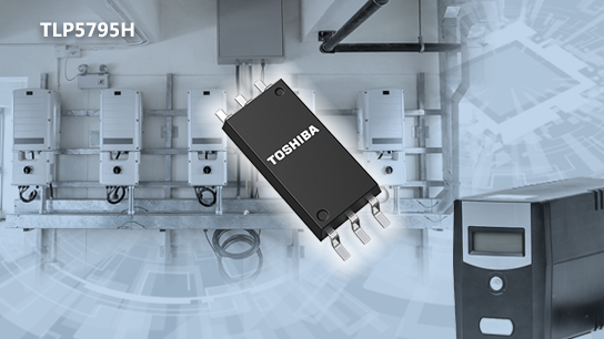
东芝电子元件及存储装置株式会社(东芝)推出了适用于中小容量MOSFET和IGBT的新款光耦TLP5795H,扩充了产品阵容,从而支持1A至5A级栅极驱动电流。该产品现已开始发货。

近年来,随着绿色能源和工厂自动化市场的扩展,从低压控制侧到高压功率器件进行隔离驱动的隔离式栅极驱动器件的需求不断增长。在这些市场中,对能够更准确地反映隔离式栅极驱动器件驱动性能的规格需求也在日益增加。对此,东芝发布了TLP5795H,其输出电流特性IOLH和IOHL为-4.5/+5.3A(典型值)。此外,东芝还在开发[1]-6.0/+4.0A(典型值)的 TLP5794H和-1.0/+1.0A(典型值)的TLP5791H。

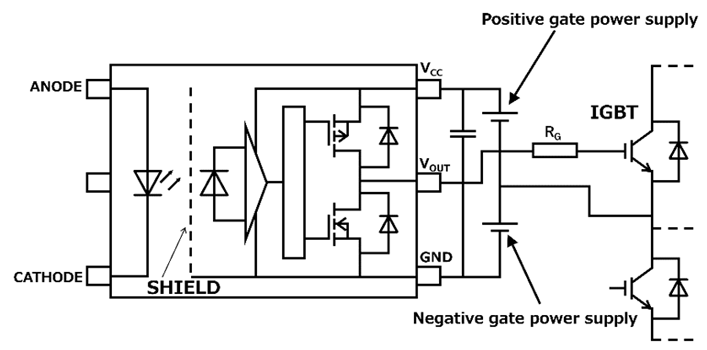
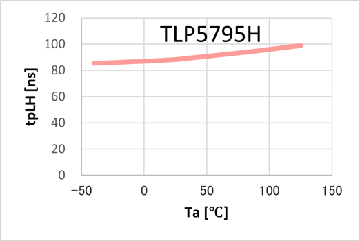
TLP5795H 的峰值高电平/低电平输出电流(IOLH/IOHL)为-4.5/+5.3A,UVLO[2]阈值电压(VUVLO+)的最大值为13.5V,UVLO阈值电压(VUVLO-)的最小值为11.1V,UVLO迟滞电压(UVLOHYS)的典型值为1.0V。这些参数为驱动具有宽栅极负偏压额定值的SiC MOSFET以及IGBT而设计。此产品适用于驱动栅极正偏压为15至20V、负偏压约为0至-10V的功率器件。详细信息,请参阅“Gate Drive Coupler Notes on using power device gate negative bias power supply”。其输出延迟时间对温度的依赖性较低,可在工厂自动化设备的实际工作范围内稳定运行。

此外,TLP5795H是一款轨对轨[3]输出器件,可实现更小电源电压下降的开关特性。

此外,东芝还通过提高输入侧红外发光二极管的光输出以及优化光接收元件(光电二极管阵列)的设计,增强了光耦合效率,实现了-40℃至125℃的工作温度范围。因此,此产品能够应用于在恶劣高温环境下运行的工业设备,例如光伏逆变器、UPS[4]和电动车充电桩。工作温度范围内的传输延迟时间和传输延迟偏差也实现了标准化。

TLP5795H采用小型SO6L封装,有助于提高电路板上元器件布局的灵活性。此外,此产品还具有8.0mm的最小爬电距离和5000Vrms的绝缘耐压,能够应用于需要高绝缘性能的设备。

东芝将继续对用于工业设备的MOSFET和IGBT栅极驱动电路的光耦产品线进行开发和扩展。

图1:IGBT栅极驱动电路示例
图1:IGBT栅极驱动电路示例

注:
[1]TLP5794H和TLP5791H计划于2025年6月发布。
[2]UVLO:欠压锁定,防止在低电压下发生故障的功能。
[3]轨对轨:输出电压能够覆盖整个电源电压范围(从正电源轨到负电源轨)的能力,适用于需要电路在低电压下工作或处理整个电源电压范围信号的应用。
[4]UPS:不间断电源。

特点

  1. UVLO compatible with SiC MOSFETs: 13.5V (max)
  2. Stable propagation delay time
  3. Rail to rail output[3]

Features Explanation

  1. 适用于SiC MOSFET的UVLO:13.5V(最大值)
  2. 稳定的传输延迟时间
  3. 轨对轨输出[3]

特性说明

1.适用于SiC MOSFET的UVLO:13.5V(最大值)

图2: UVLO迟滞对比
图2: UVLO迟滞对比

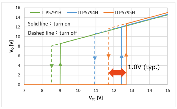
可设置高栅极电压,使其适用于大功率应用。此外,通过1.0V(典型值)的迟滞电压稳定输出,提高了系统的整体可靠性。

2.稳定的传输延迟时间

Figure 2. UVLO hysteresis comparison

High gate voltage can be set, making it suitable for high-power applications. Additionally, the output is stabilized with a hysteresis of 1.0V (typ.), improving the overall reliability of the system.

2. Stable propagation delay time

The propagation delay time of TLP5795H is stable within the operating temperature rating of -40 to 125°C.
Moreover, it operates stably within the practical range defined by FA equipment.

Figure 3. Temperature characteristics of propagation delay time (tpLH)
Figure 4. Temperature characteristics of propagation delay time (tpHL)

3. Rail to rail output[3]

Rail to rail output allows the output voltage to be used within the range of power supply voltage.
In addition, due to the low internal resistance of the gate driver coupler, it results in low loss.
This minimizes switching losses and improves efficiency of equipment.

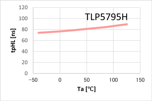
TLP5795H的输出延迟时间在-40℃至125℃的工作温度范围内保持稳定。
此外,它在工厂自动化设备的实际工作范围内也能稳定运行。

3.轨对轨输出[3]

轨对轨输出允许在电源电压范围内使用输出电压。
此外,由于栅极驱动光耦的内部电阻较低,因此损耗也较低。
这样,最大限度地减少了开关损耗,提高了设备的效率。

应用

  • PV Inverters
  • UPS
  • EV charger stand
  • Inverter drive
  • IH cooking heaters
  • Air conditioners
  • 光伏逆变器
  • UPS
  • 电动车充电桩
  • 逆变器驱动电路
  • IH电磁炉
  • 空调

主要规格

(Unless otherwise specified, Ta = -40 to 125°C)

Part number

TLP5795H

TLP5794H[1]

TLP5791H[1]

Package

Name

SO6L

Size (mm)

Typ.

3.84×10×2.1

Recommended
Operating
Conditions

Peak high-level/low-level output current

(L/H) IOLH, (H/L) IOHL (A)

-4.5/+5.3

-6.0/+4.0

-1/+1

Supply voltage VCC (V)

15 to 30

15 to 30

10 to 30

Electrical characteristics

UVLO threshold voltage

VUVLO+ (V)

IF=5mA, VO>2.5V

Max

13.5

13.5

9.5

UVLO threshold voltage

VUVLO- (V)

IF=5mA, VO<2.5V

Min

11.1

9.5

7.5

UVLO hysteresis

UVLOHYS (V)

-

Typ.

1.0

1.5

0.5

Switching characteristics

Propagation delay time

(L/H) tpLH, (H/L) tpHL (ns)

VCC=30V

Max

150

200

500

High-level/Low-level common-mode transient immunity

CMH, CML (kV/μs)

Ta=25°C

Min

±35

±50

±20

Isolation characteristics

Isolation voltage BVS (Vrms)

Ta=25°C

Min

5000

Buy Online

Buy Online

-

-

(除非另有规定,Ta=-40至125℃)

器件型号

TLP5795H

TLP5794H[1]

TLP5791H[1]

封装

名称

SO6L

尺寸(mm)

典型值

3.84×10×2.1

建议的工作条件

峰值高电平/低电平输出电流

(L/H)IOLH,(H/L)IOHL(A)

-4.5/+5.3

-6.0/+4.0

-1/+1

电源电压VCC(V)

15至30

15至30

10至30

电气特性

UVLO阈值电压

VUVLO+(V)

IF=5mA,VO>2.5V

最大值

13.5

13.5

9.5

UVLO阈值电压

VUVLO-(V)

IF=5mA,VO<2.5V

最小值

11.1

9.5

7.5

UVLO迟滞

UVLOHYS(V)

-

典型值

1.0

1.5

0.5

开光特性

传输延迟时间

(L/H)tpLH,(H/L)tpHL(ns)

VCC=30V

最大值

150

200

500

高电平/低电平共模瞬态抑制

CMH,CML(kV/μs)

Ta=25°C

最小值

±35

±50

±20

绝缘特性

绝缘耐压BVS(Vrms)

Ta=25°C

最小值

5000

库存查询与购买

Buy Online

-

-

联系我们

技术咨询

联系我们

联系我们

常见问题

常见问题(FAQ)

Queries about purchasing, sampling and IC reliability

购买、样品、及IC可靠性查询

库存查询与购买

keyword:

Disclaimer for External Link
Through this website you are able to proceed to the website of our distributors ("Third Party Website") which is not under the control of Toshiba Corporation and its subsidiaries and affiliates (collectively "Toshiba"). The Third Party Website is made available to you as a convenience only and you agree to use the Third Party Website at your own risk. The link of the Third Party Website does not necessarily imply a recommendation or an endorsement by Toshiba of the Third Party Website. Please be aware that Toshiba is not responsible for any transaction done through the Third Party Website, and such transactions shall be subject to terms and conditions which may be provided in the Third Party Website.

*本文提及的公司名称、产品名称和服务名称可能是其各自公司的商标。
*本文件中所含信息,包括产品价格和产品规格、服务内容及联系方式,仅于公告当日有效,如有更改,恕不另行通知。

在新窗口打开