- 型号 & 关键词搜索
- 交叉搜索
- 参数搜索
- 库存查询与购买
This webpage doesn't work with Internet Explorer. Please use the latest version of Google Chrome, Microsoft Edge, Mozilla Firefox or Safari.
请输入3个以上字符 Search for multiple part numbers fromhere.
The information presented in this cross reference is based on TOSHIBA's selection criteria and should be treated as a suggestion only. Please carefully review the latest versions of all relevant information on the TOSHIBA products, including without limitation data sheets and validate all operating parameters of the TOSHIBA products to ensure that the suggested TOSHIBA products are truly compatible with your design and application.Please note that this cross reference is based on TOSHIBA's estimate of compatibility with other manufacturers' products, based on other manufacturers' published data, at the time the data was collected.TOSHIBA is not responsible for any incorrect or incomplete information. Information is subject to change at any time without notice.
请输入3个以上字符
低辐射发射噪声
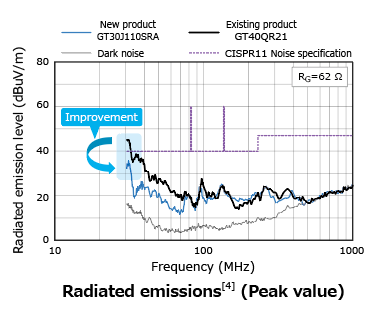
优化的芯片设计可实现低辐射发射噪声。通常,较低的外部栅极电阻(RG)降低关断开关损耗并提高辐射的发射噪声。通过改善关断开关损耗和辐射发射噪声之间的平衡,可降低开关损耗。
辐射发射噪声低

新产品的辐射发射噪声在大约30MHz(噪声场强最强处)时改善了大约10dBμV/m。

