


- 型号 & 关键词搜索
- 交叉搜索
- 参数搜索
- 库存查询与购买
This webpage doesn't work with Internet Explorer. Please use the latest version of Google Chrome, Microsoft Edge, Mozilla Firefox or Safari.
请输入3个以上字符 Search for multiple part numbers fromhere.
The information presented in this cross reference is based on TOSHIBA's selection criteria and should be treated as a suggestion only. Please carefully review the latest versions of all relevant information on the TOSHIBA products, including without limitation data sheets and validate all operating parameters of the TOSHIBA products to ensure that the suggested TOSHIBA products are truly compatible with your design and application.Please note that this cross reference is based on TOSHIBA's estimate of compatibility with other manufacturers' products, based on other manufacturers' published data, at the time the data was collected.TOSHIBA is not responsible for any incorrect or incomplete information. Information is subject to change at any time without notice.
请输入3个以上字符
具有MOSFET栅极驱动IC和N沟道MOSFET的负载开关电路示例
东芝的栅极驱动电路IC与MOSFET组合后,实现了具有保护功能的平滑导通和关断负载开关。利用共漏极MOSFET,该解决方案实现了具有反向电流阻断功能的小型低损耗输电线。
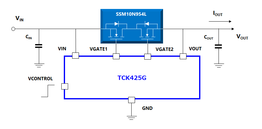
下面显示了TCK425G与SSM10N954L在5V输电线中的组合示例。
| 器件型号 | 特性 |
|---|---|
| TCK425G | 过压保护MOSFET栅极驱动IC 栅极-源极电压:VGS=5.6V(典型值) 过压锁定:VIN_OVLO=6.31V(典型值) 封装:WCSP6G |
| SSM10N954L | 共漏极N沟道MOSFET 源极-源极电压:VSSS=12V(最大值) 栅极-源极电压:±8V(最大值) 源极-源极导通电阻:当VGS=4.5V时,为2.1mΩ(典型值) 封装:TCSPAC-153001 |

无任何浪涌电流、输出电压过冲和欠冲的平滑导通和关断波形。
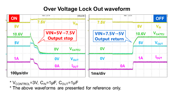
集成了过压锁定(OVLO)功能,可保护过压电源。当输入电压超过OVLO阈值时,OVLO功能会立即关闭输出。当输入电压降至OVLO阈值以下之后,输出开启。
MOSFET栅极驱动IC
推荐MOSFET
文档
相关信息
购买、样品、及IC可靠性查询
库存查询与购买
请输入3个以上字符
Through this website you are able to proceed to the website of our distributors ("Third Party Website") which is not under the control of Toshiba Corporation and its subsidiaries and affiliates (collectively "Toshiba"). The Third Party Website is made available to you as a convenience only and you agree to use the Third Party Website at your own risk. The link of the Third Party Website does not necessarily imply a recommendation or an endorsement by Toshiba of the Third Party Website. Please be aware that Toshiba is not responsible for any transaction done through the Third Party Website, and such transactions shall be subject to terms and conditions which may be provided in the Third Party Website.