


- 型号 & 关键词搜索
- 交叉搜索
- 参数搜索
- 库存查询与购买
This webpage doesn't work with Internet Explorer. Please use the latest version of Google Chrome, Microsoft Edge, Mozilla Firefox or Safari.
请输入3个以上字符 Search for multiple part numbers fromhere.
The information presented in this cross reference is based on TOSHIBA's selection criteria and should be treated as a suggestion only. Please carefully review the latest versions of all relevant information on the TOSHIBA products, including without limitation data sheets and validate all operating parameters of the TOSHIBA products to ensure that the suggested TOSHIBA products are truly compatible with your design and application.Please note that this cross reference is based on TOSHIBA's estimate of compatibility with other manufacturers' products, based on other manufacturers' published data, at the time the data was collected.TOSHIBA is not responsible for any incorrect or incomplete information. Information is subject to change at any time without notice.
请输入3个以上字符
车载MOSFET的封装趋势
封装技术趋势
功率MOSFET封装技术趋势
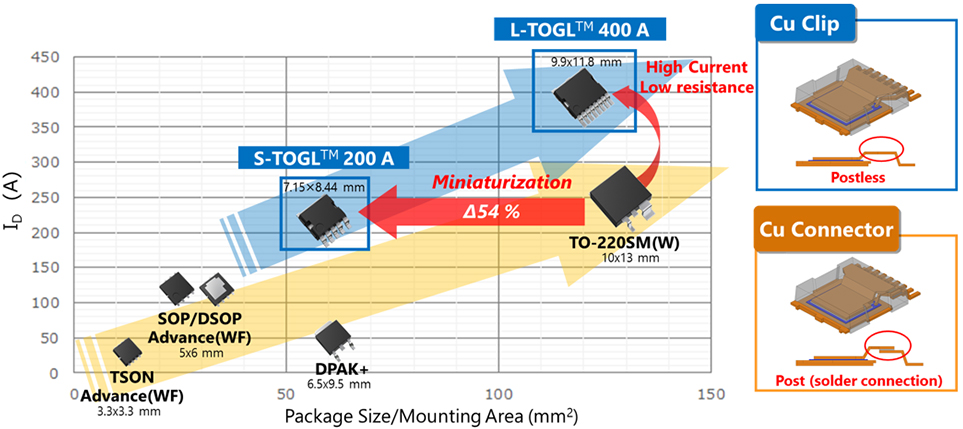
DPAK+、DSOP Advance(WF)、SOP Advance(WF)和TSON Advance(WF)采用铜连接器结构,实现了高电流导通能力。此外,S-TOGL™和L-TOGL™新型封装通过将铜连接器结构演变为铜夹结构(内部无柱结构)和采用多引脚结构,从而实现了更高的电流导通能力。此外,目前正在开发的SOF-Dual与使用两个SOP Advance(WF)单元相比,安装面积减少了约40%。这有助于小型化。我们正在扩大我们的产品线,以满足车载应用的不同需求。
小封装技术趋势

小型MOSFET提供了广泛的击穿电压和驱动电压范围,涵盖小信号到中功率类型。封装尺寸有多种选择,从1mm×1mm超级小封装到3mm×3mm,通过减少安装面积促进设备小型化。
车载MOSFET
相关信息
购买、样品、及IC可靠性查询
库存查询与购买
请输入3个以上字符
Through this website you are able to proceed to the website of our distributors ("Third Party Website") which is not under the control of Toshiba Corporation and its subsidiaries and affiliates (collectively "Toshiba"). The Third Party Website is made available to you as a convenience only and you agree to use the Third Party Website at your own risk. The link of the Third Party Website does not necessarily imply a recommendation or an endorsement by Toshiba of the Third Party Website. Please be aware that Toshiba is not responsible for any transaction done through the Third Party Website, and such transactions shall be subject to terms and conditions which may be provided in the Third Party Website.
*S-TOGL™、L-TOGL™是东芝电子元件及存储装置株式会社的商标。
*本文提及的公司名称,产品名称和服务名称可能是其各自公司的商标。