


- 型号 & 关键词搜索
- 交叉搜索
- 参数搜索
- 库存查询与购买
This webpage doesn't work with Internet Explorer. Please use the latest version of Google Chrome, Microsoft Edge, Mozilla Firefox or Safari.
请输入3个以上字符 Search for multiple part numbers fromhere.
The information presented in this cross reference is based on TOSHIBA's selection criteria and should be treated as a suggestion only. Please carefully review the latest versions of all relevant information on the TOSHIBA products, including without limitation data sheets and validate all operating parameters of the TOSHIBA products to ensure that the suggested TOSHIBA products are truly compatible with your design and application.Please note that this cross reference is based on TOSHIBA's estimate of compatibility with other manufacturers' products, based on other manufacturers' published data, at the time the data was collected.TOSHIBA is not responsible for any incorrect or incomplete information. Information is subject to change at any time without notice.
请输入3个以上字符
采用新高击穿电压SOI工艺降低损耗
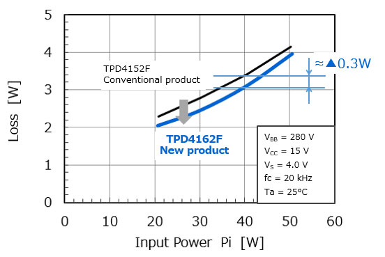
单片方波驱动产品采用新高击穿电压SOI(绝缘硅)工艺。功率IC配备了600伏IGBT、续流二极管(FWD)和控制电路。功率IC安装在与低热阻外露焊盘(E-Pad)兼容的封装(HSSOP31)上。采用少量外围部件即可以驱动小型高效无刷电机。在东芝最新的产品中,开关损耗降低,从而比传统产品的效率提高约0.3W。
新产品采用新高击穿电压SOI工艺,与传统产品相比,降低了开关损耗,提高效率约0.3W(@输入功率=40W)。
除了传统的限流功能外,我们还增加了过电流保护功能,以提高系统故障的安全性,例如当电机锁定时。霍尔元件可以作为检测转子位置的传感器,有助于降低系统成本。
单片3相直流无刷电机驱动IC
相关信息
购买、样品、及IC可靠性查询
库存查询与购买
请输入3个以上字符
Through this website you are able to proceed to the website of our distributors ("Third Party Website") which is not under the control of Toshiba Corporation and its subsidiaries and affiliates (collectively "Toshiba"). The Third Party Website is made available to you as a convenience only and you agree to use the Third Party Website at your own risk. The link of the Third Party Website does not necessarily imply a recommendation or an endorsement by Toshiba of the Third Party Website. Please be aware that Toshiba is not responsible for any transaction done through the Third Party Website, and such transactions shall be subject to terms and conditions which may be provided in the Third Party Website.