TRS12V65H

SiC Schottky barrier diode

  • 相关参考设计(1)

产品概要

Application Scope Power factor correction / Solar inverters / Uninterruptible power supplies / DC-DC converters
Feature Chip design of 3rd generation
Number of Circuits 1
Internal Connection Single
RoHS Compatible Product(s) (#) Available

封装

Toshiba Package Name DFN 8×8
Package Image 东芝 TRS12V65H SiC Schottky barrier diode产品 DFN 8×8 封装图片
Pins 5
Mounting Surface Mount
Width×Length×Height
(mm)
8.0×8.0×0.85
Package Dimensions 查看
Land pattern dimensions 查看
Ultra Librarian® CAD model
(Symbol, Footprint and 3D model)
Download from UltraLibrarian<sup>®</sup> in your desired CAD format<br>(Note1)(Note3)

Download from UltraLibrarian® in your desired CAD format
(Note1)(Note3)

SamacSys CAD model
(Symbol, Footprint and 3D model)
Download from SamacSys<br>(Note2)(Note3)

Download from SamacSys
(Note2)(Note3)

 Please refer to the link destination to check the detailed size.

(Note1)

Ultra Librarian® is a Registered trademark and CAD model library of EMA (EMA Design Automation, Inc.). CAD models (Symbol/Footprint /3D model) are provided by UltraLibrarian®. The footprints are generated based on the specifications of Ultra Librarian®.

(Note2)

SamacSys is a wholly owned subsidiary of Supplyframe, Inc. CAD models (Symbol/Footprint /3D model) are provided by Supplyframe, Inc. The footprints are generated based on the specifications of SamacSys.

(Note3)

Please note that the footprint dimensions may differ from the reference Land Pattern dimensions provided on our website.

绝对最大额定值

项目 符号 单位
Forward DC current IF(DC) 12 A
Repetitive Peak Reverse Voltage VRRM 650 V

电气特性

项目 符号 条件 单位
Reverse current (Max) IR VRRM=650V 120 μA
Forward Voltage (Max) VF IF=12A 1.35 V
Forward Voltage (Typ.) VF IF=12A 1.2 V
购买及样品申请
请联系东芝官方代理商或就近联系我们的销售网点。
您可以通过以下链接搜索及购买少量样品。

文档

  • 如果该复选框不能被选中,则不能批量下载相应的文档。

Feb,2024

Feb,2024

Feb,2024

Mar,2025

Jul,2025

(Note1)

LTspice ® is a trademark and simulation software of ADI (Analog Devices, Inc.).

(Note2)

SIMetrix® is simulation software and registered trademarks of SIMetrix Technologies Ltd.

参考设计

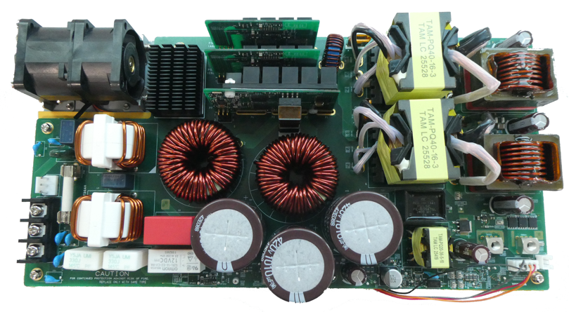
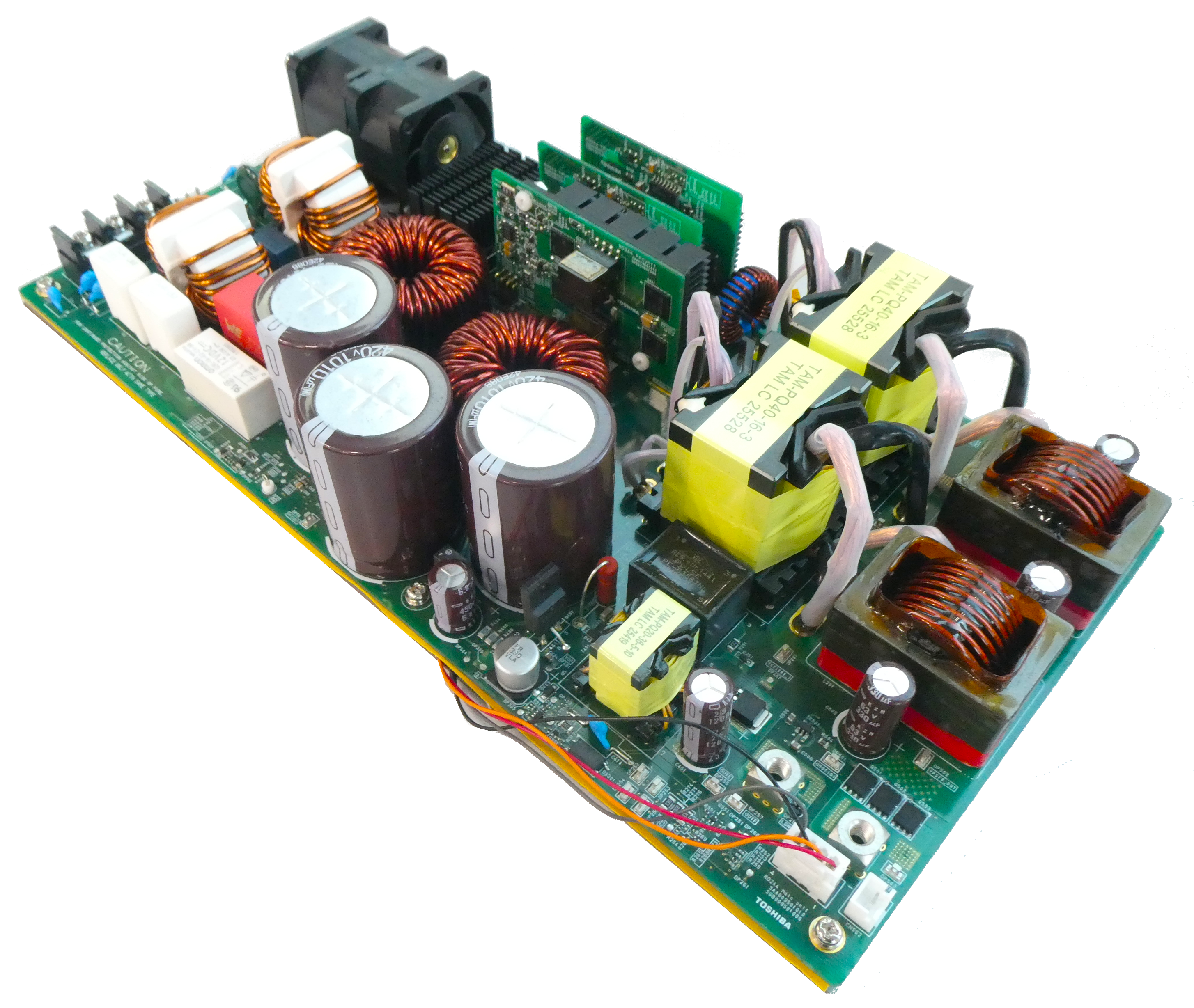
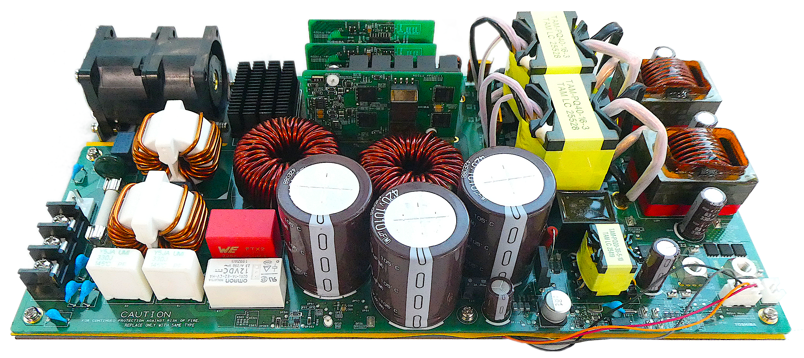
采用表贴式SiC MOSFET的3kW服务器及通信电源
近年来,数据中心规模不断扩大,密度不断提升。因此,服务器电源也需要更高效、更强大、更节省空间,高功率密度至关重要。我们采用最新的表面贴装SiC器件,将电源从主板分离,并将其作为子板实现,从而实现了高功率密度。
除了服务器应用外,该解决方案还适用于通信系统和其他使用48V的应用。
本参考设计提供了电路各部分的设计要点、使用方法和调整方法的说明,以及电路图、电路板布局等设计信息,可为您的设计提供帮助。
3kW Power Supply for AI Servers Using Surface-Mounted SiC MOSFET
With the rapid rise of generative AI, demand for high-performance AI servers is growing. This reference design provides a 3kW power supply for AI servers with high power requirements. By incorporating our surface-mount SiC MOSFETs, it achieves high power density.
Design tips on each portion of the circuit, method of operation, and design information such as circuit diagrams and PCB patterns are available, please use them for your design.
3kW Power Supply for Electric Scooter Fast Chargers Using SiC MOSFET
In recent years, the growing focus on carbon neutrality has led to increased popularity of electric scooters, driving demand for fast battery charging. This reference design presents a 3kW power supply tailored for fast chargers used with electric scooters.
Design tips on each portion of the circuit, method of operation, and design information such as circuit diagrams and PCB patterns are available, please use them for your design.

应用

变频器/伺服
在设计变频器/伺服时,低功耗、小型化和稳定运行等非常重要。东芝提供适用于电源单元、电机驱动电路单元、信号传输单元等的各种半导体产品的信息以及电路配置示例。
服务器
在设计服务器时,低功耗和小型化等非常重要。东芝提供了适用于电源单元、电机驱动单元、过温监控单元等的各种半导体产品的信息以及电路配置示例。
IoT传感器
低功耗和小型化等对于IoT传感器的设计非常重要的。东芝提供了适用于电源单元、传感器信号输入单元、控制单元、显示单元等的各种半导体产品的信息以及电路配置示例。
不间断电源
在设计不间断电源(UPS)时,低功耗和小型化等非常重要。东芝提供适用于电源单元、逆变器/转换器单元、控制单元、信号传输单元等的各种半导体产品的信息以及电路配置示例。
温控器
在设计温控器时,低功耗和小型化等非常重要。东芝提供适用于电源单元、隔离单元、传感器信号输入单元等的各种半导体产品的信息以及电路配置示例。

技术咨询

联系我们

联系我们

常见问题

常见问题(FAQ)

Notes

返回列表页
在新窗口打开