


- 型号 & 关键词搜索
- 交叉搜索
- 参数搜索
- 库存查询与购买
This webpage doesn't work with Internet Explorer. Please use the latest version of Google Chrome, Microsoft Edge, Mozilla Firefox or Safari.
请输入3个以上字符 Search for multiple part numbers fromhere.
The information presented in this cross reference is based on TOSHIBA's selection criteria and should be treated as a suggestion only. Please carefully review the latest versions of all relevant information on the TOSHIBA products, including without limitation data sheets and validate all operating parameters of the TOSHIBA products to ensure that the suggested TOSHIBA products are truly compatible with your design and application.Please note that this cross reference is based on TOSHIBA's estimate of compatibility with other manufacturers' products, based on other manufacturers' published data, at the time the data was collected.TOSHIBA is not responsible for any incorrect or incomplete information. Information is subject to change at any time without notice.
请输入3个以上字符
MOSFET漏极-源极导通电阻RDS(ON)是什么?
是指当MOSFET在指定的栅极电压下导通时漏极与源极之间的电阻。
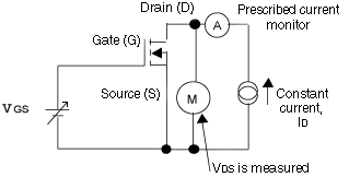
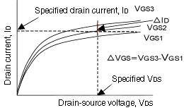
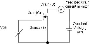
要测量漏极-源极电阻(RDS(ON)),首先要在栅极和源极之间施加一个超过指定阈值电压(Vth)的电压。然后,施加指定的电流源(ID)并测量漏极和源极之间的压降(VDS)。
利用这些测量值,您可以使用公式计算出指定栅极-源极电压(VGS)的RDS(ON)值:RDS(ON)=VDS/ID。
注)确保恒流电源的开路电压等于或小于漏极与地之间的耐压。
相关信息也请参考以下页面。