- 型号 & 关键词搜索
- 交叉搜索
- 参数搜索
- 库存查询与购买
This webpage doesn't work with Internet Explorer. Please use the latest version of Google Chrome, Microsoft Edge, Mozilla Firefox or Safari.
请输入3个以上字符 Search for multiple part numbers fromhere.
The information presented in this cross reference is based on TOSHIBA's selection criteria and should be treated as a suggestion only. Please carefully review the latest versions of all relevant information on the TOSHIBA products, including without limitation data sheets and validate all operating parameters of the TOSHIBA products to ensure that the suggested TOSHIBA products are truly compatible with your design and application.Please note that this cross reference is based on TOSHIBA's estimate of compatibility with other manufacturers' products, based on other manufacturers' published data, at the time the data was collected.TOSHIBA is not responsible for any incorrect or incomplete information. Information is subject to change at any time without notice.
请输入3个以上字符
什么是总线开关?
总线开关是一种对传输数字信号进行优化的半导体开关。总线开关的基本功能与机械开关相同,采用MOSFET来实现开/关功能(图1)。
总线开关只是一个开关:与缓冲器不同,它不能驱动负载。总线开关专为高速数字信号传输而设计,用于导通和关断信号流或在输出端口之间开关。
东芝不仅提供简易型单刀单掷(SPST)开关,还可提供单刀双掷(SPDT)和单刀四掷(SP4T)多路复用器。
用于打开和关闭电源轨的半导体开关大致分为信号开关和负载开关(负载开关IC)。下面介绍信号开关。
信号开关有两种类型:处理数字信号的开关和处理模拟信号的开关。
总线开关专门用于传输数字信号。对于数字信号,必须以低延时或无延时的方式传输其逻辑状态(包括电压电平)。相反,模拟开关需要信号线性。换言之,低电容和导通电阻对于总线开关很重要,而模拟开关需要在信号传输的电压范围内很低且恒定的导通电阻。
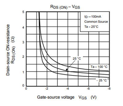
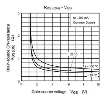
通常,用于开关应用的p沟道和n沟道MOSFET的导通电阻取决于控制电压以及通过开关的信号的电压,如图2和图3所示。为补偿这种电压依赖性,模拟开关由并联的p沟道和n沟道MOSFET组成,如图4所示。这使其导通电阻在工作电压范围内保持恒定,但开关电容会相应增大。
相反,总线开关仅由一个p沟道MOSFET构成(或N沟道MOSFET)组成,如图 5 所示。虽然其导通电阻也取决于电压,但此电压足够低,故不会干扰数字信号传输。.
因此,总线开关是高速数字传输的理想之选。如欲传输模拟信号,请使用具有模拟电气特性的模拟开关。


相关链接
以下文档也包含相关链接。