- 型号 & 关键词搜索
- 交叉搜索
- 参数搜索
- 库存查询与购买
This webpage doesn't work with Internet Explorer. Please use the latest version of Google Chrome, Microsoft Edge, Mozilla Firefox or Safari.
请输入3个以上字符 Search for multiple part numbers fromhere.
The information presented in this cross reference is based on TOSHIBA's selection criteria and should be treated as a suggestion only. Please carefully review the latest versions of all relevant information on the TOSHIBA products, including without limitation data sheets and validate all operating parameters of the TOSHIBA products to ensure that the suggested TOSHIBA products are truly compatible with your design and application.Please note that this cross reference is based on TOSHIBA's estimate of compatibility with other manufacturers' products, based on other manufacturers' published data, at the time the data was collected.TOSHIBA is not responsible for any incorrect or incomplete information. Information is subject to change at any time without notice.
请输入3个以上字符
SBD的正向电压(VF)是什么?
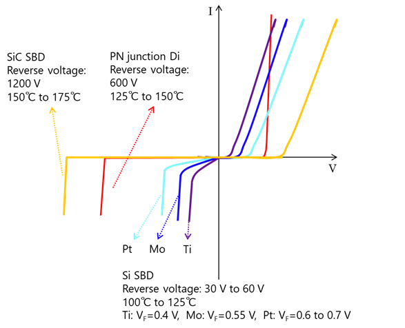
根据所使用的金属,SBD的额定正向电压(VF)介于0.4 V至0.7 V之间,低于pn结二极管的正向电压。然而,硅肖特基势垒二极管的耐压为20V至150 V,不高于pn结二极管的耐压。
东芝还提供采用宽禁带(WBG)半导体(SiC)制造的SBD,该半导体具有高击穿电场,可承受高达650V的电压。
图1比较了无偏状态下pn结二极管和SBD的能带图。pn结二极管的正向电压(VF)取决于p型与n型半导体之间的势能差,而SBD的正向电压(VF)取决于金属的功函数与硅等材质的n型半导体(即肖特基势垒)的电子亲和力之差。因此,可通过使用功函数接近n型半导体(例如,硅)电子亲和力的金属,构建具有低VF的SBD。图2显示了VF的差异,具体取决于所使用的金属。


相关链接
关于产品,请参考以下链接


