


- 型号 & 关键词搜索
- 交叉搜索
- 参数搜索
- 库存查询与购买
This webpage doesn't work with Internet Explorer. Please use the latest version of Google Chrome, Microsoft Edge, Mozilla Firefox or Safari.
请输入3个以上字符 Search for multiple part numbers fromhere.
The information presented in this cross reference is based on TOSHIBA's selection criteria and should be treated as a suggestion only. Please carefully review the latest versions of all relevant information on the TOSHIBA products, including without limitation data sheets and validate all operating parameters of the TOSHIBA products to ensure that the suggested TOSHIBA products are truly compatible with your design and application.Please note that this cross reference is based on TOSHIBA's estimate of compatibility with other manufacturers' products, based on other manufacturers' published data, at the time the data was collected.TOSHIBA is not responsible for any incorrect or incomplete information. Information is subject to change at any time without notice.
请输入3个以上字符
SiC SBD的高耐压(反压)特性
碳化硅(SiC)是一种宽带隙半导体,其带隙宽度为3.26eV,远高于硅(Si)的带隙宽度(=1.12eV)。SiC具有较高的击穿电场和较高的热导率,这是由于它具有较低的晶格常数(即较短的原子间距离)从而具有较高的原子键。
Si和SiC的物理性质比较
| 特性 | 单位 | Si | 4H-SiC |
|---|---|---|---|
| 带隙 | eV | 1.12 | 3.26 |
| 电子迁移率,μe | cm2/Vs | 1400 | 1000/1200 |
| 空穴迁移率,μh | 600 | 120 | |
| 击穿电场,Ec | V/cm | 3.0×10⁵ | 2.8×10⁶ |
| 热导率,λ | W/cmK | 1.5 | 4.9 |
| 饱和电子漂移速度,Vsat | cm/s |
1.0×10⁷ | 2.2×10⁷ |
| 相对介电常数,ε | 11.8 | 9.7/10.2 |
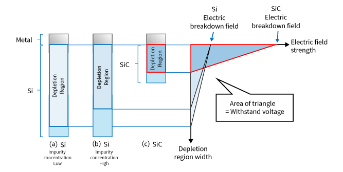
当具有传统结构的SBD反向偏压时,耗尽区将延伸到半导体中,如下所示。由击穿电场和耗尽区宽度形成的三角形区域代表SBD耐受电压。耗尽区深度与掺杂浓度成反比。提高掺杂浓度有助于降低硅的电阻,从而降低SBD正向电压(VF),但要牺牲耐受电压(即三角形区域)。碳化硅的击穿电场几乎是硅的10倍。因此,如下图所示,即使SiC SBD是重掺杂的,也可以增加SiC SBD相对于Si SBD的耐受电压(即三角形区域)。
此外,由于耗尽层因较高浓度而拉伸较小,因此芯片的厚度将小于采用Si的情况。半导体(Si或SiC)的厚度可以看作是正向的串联电阻,因此可以通过减小厚度来提高正向电压。
SiC肖特基二极管
相关信息
购买、样品、及IC可靠性查询
库存查询与购买
请输入3个以上字符
Through this website you are able to proceed to the website of our distributors ("Third Party Website") which is not under the control of Toshiba Corporation and its subsidiaries and affiliates (collectively "Toshiba"). The Third Party Website is made available to you as a convenience only and you agree to use the Third Party Website at your own risk. The link of the Third Party Website does not necessarily imply a recommendation or an endorsement by Toshiba of the Third Party Website. Please be aware that Toshiba is not responsible for any transaction done through the Third Party Website, and such transactions shall be subject to terms and conditions which may be provided in the Third Party Website.