- 型号 & 关键词搜索
- 交叉搜索
- 参数搜索
- 库存查询与购买
This webpage doesn't work with Internet Explorer. Please use the latest version of Google Chrome, Microsoft Edge, Mozilla Firefox or Safari.
请输入3个以上字符 Search for multiple part numbers fromhere.
The information presented in this cross reference is based on TOSHIBA's selection criteria and should be treated as a suggestion only. Please carefully review the latest versions of all relevant information on the TOSHIBA products, including without limitation data sheets and validate all operating parameters of the TOSHIBA products to ensure that the suggested TOSHIBA products are truly compatible with your design and application.Please note that this cross reference is based on TOSHIBA's estimate of compatibility with other manufacturers' products, based on other manufacturers' published data, at the time the data was collected.TOSHIBA is not responsible for any incorrect or incomplete information. Information is subject to change at any time without notice.
请输入3个以上字符
What should be noted when setting SiC MOSFET gate voltage (VGS)?
The precautions for setting VGS are explained referring to Toshiba’s SiC MOSFET TW060Z120C.
i) Within the absolute maximum ratings
Use VGS within the absolute maximum rated VGS=+25,-10V including the surge voltage and considering the derating.
ii) Set VGS at turn-on to 18V or higher
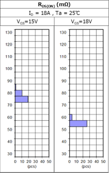
A disribution map of the on-resistance (RDS(ON)) is shown in Figure 1. In VGS=15V map shown on the left, the on-resistance increases rapidly. By setting VGS to 18V or higher, the variation with low on-resistance can be reduced.

iii) Set the gate voltage at turn-off to 0V or less
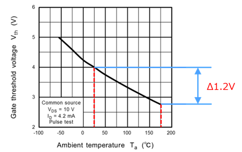
Vth – Ta curve is shown in Figure 2. The lower limit of gate threshold voltage (Vth) is 3.0V at Ta=25°C. In addition, as shown in the temperature characteristic curve, Vth has a negative temperature coefficient and drops 1.2V at 25°C ⇒ 175°C. Confirm the gate voltage does not exceed Vth and not be turned on incorrectly during the off-period due to the voltage fluctuations during actual operation.

iv) Charge the gate-source capacitance sufficiently with the gate charge.
The gate-source capacitance must be charged with gate charges to rise VGS to turn on. For TW060Z120C, the gate charge at VGS =18V is typically 46nC as shown in Table1. Apply the gate current that can sufficiently charge the gate charge at the frequency to be used.
| Characteristics | Symbol | Test Condition | Min | Тур. | Мах | Unit |
|---|---|---|---|---|---|---|
| Total gate charge (gate-source plus gate-drain) | Qg | VDD ≈ 800V, VGS = 18V, ID = 18A | - | 46 | - | nC |
| Gate-source charge 1 | Qgs1 | - | 18 | - | ||
| Gate-drain charge | Qgd | - | 7.8 | - |
Table 1. Gate charge characteristics in data sheet @Ta=25℃ (TW060Z120C)
Related links
The following documents also contain related information.


