- 型号 & 关键词搜索
- 交叉搜索
- 参数搜索
- 库存查询与购买
This webpage doesn't work with Internet Explorer. Please use the latest version of Google Chrome, Microsoft Edge, Mozilla Firefox or Safari.
请输入3个以上字符 Search for multiple part numbers fromhere.
The information presented in this cross reference is based on TOSHIBA's selection criteria and should be treated as a suggestion only. Please carefully review the latest versions of all relevant information on the TOSHIBA products, including without limitation data sheets and validate all operating parameters of the TOSHIBA products to ensure that the suggested TOSHIBA products are truly compatible with your design and application.Please note that this cross reference is based on TOSHIBA's estimate of compatibility with other manufacturers' products, based on other manufacturers' published data, at the time the data was collected.TOSHIBA is not responsible for any incorrect or incomplete information. Information is subject to change at any time without notice.
请输入3个以上字符
What are the characteristics of body diode in SiC MOSET?
A body diode in a general SiC MOSFET is a SiC pn junction diode. The reverse recovery time (trr) of this pn junction diode is faster than that of a normal Si pn junction diode.
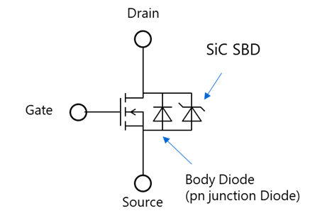
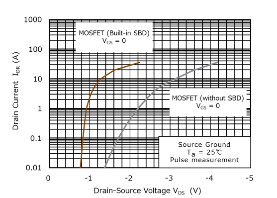
As shown in Figure 1, Toshiba’s third generation SiC MOSFET has a built-in SiC Schottky barrier diode (SBD) between SiC MOSFET’s drain and source. This reduces the inductance due to wires and circuit boards when the SBD is connected externally. Threfore Toshiba’s third generation SiC MOSFET is a suitable device for reducing the losses and noises caused by high frequency switching. In addition, the forward voltage (VF) is smaller than that of SiC MOSFET without a built-in SBD, and conduction loss can be reduced as shown in Figure 2.
Built-in SBD is also effective for improving reliability. As mentioned above, Toshiba’s SiC MOSFET has a built-in SiC SBD and is designed to be less conductive to the body diode (pn junction diode). This reduces the risk of variations in characteristics such as the forward voltage of pn junction diode (VF), the threshold voltage (Vth) and the on-resistance (RDS(ON)) of SiC MOSFET, due to crystal dfects generated during long-term operation.


Related links
The following documents also contain related information.


