


- 型号 & 关键词搜索
- 交叉搜索
- 参数搜索
- 库存查询与购买
This webpage doesn't work with Internet Explorer. Please use the latest version of Google Chrome, Microsoft Edge, Mozilla Firefox or Safari.
请输入3个以上字符 Search for multiple part numbers fromhere.
The information presented in this cross reference is based on TOSHIBA's selection criteria and should be treated as a suggestion only. Please carefully review the latest versions of all relevant information on the TOSHIBA products, including without limitation data sheets and validate all operating parameters of the TOSHIBA products to ensure that the suggested TOSHIBA products are truly compatible with your design and application.Please note that this cross reference is based on TOSHIBA's estimate of compatibility with other manufacturers' products, based on other manufacturers' published data, at the time the data was collected.TOSHIBA is not responsible for any incorrect or incomplete information. Information is subject to change at any time without notice.
请输入3个以上字符
是什么驱动晶体管:电流还是电压?
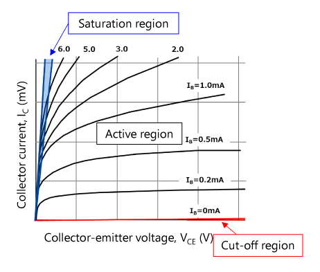
大致而言,双极晶体管会放大进入基极的小电流以产生集电极大电流。由于集电极电流是通过基极电流控制的,因此它是一个电流驱动型器件。电流增益随集电极-发射极电压(VCE)的变化而变化。在右图所示的放大工作区域内,双极晶体管提供了一个称为直流电流增益(hFE)的增益。在该区域内,集电极电流几乎保持恒定,与集电极-发射极电压(VCE)无关。另一方面,在饱和区中,双极晶体管的直流电流增益仅为10至20,其中集电极电流随VCE的变化而大幅变化。
场效应晶体管(FET)控制电流通路(称为“沟道”)的宽度,该沟道由施加在栅极和源极端子的电压产生。沟道宽度的变化会导致漏源电阻发生变化。因此,FET是一种电压驱动器件。
IGBT是在前级的MOSFET(一种场效应管(FET))与和后级的双极晶体管组合在一起的一种器件。IGBT导通时,其工作原理与FET相同。因此,IGBT也是一种电压驱动器件。
相关信息,详见e-learning第3章“晶体管”。