- 型号 & 关键词搜索
- 交叉搜索
- 参数搜索
- 库存查询与购买
This webpage doesn't work with Internet Explorer. Please use the latest version of Google Chrome, Microsoft Edge, Mozilla Firefox or Safari.
请输入3个以上字符 Search for multiple part numbers fromhere.
The information presented in this cross reference is based on TOSHIBA's selection criteria and should be treated as a suggestion only. Please carefully review the latest versions of all relevant information on the TOSHIBA products, including without limitation data sheets and validate all operating parameters of the TOSHIBA products to ensure that the suggested TOSHIBA products are truly compatible with your design and application.Please note that this cross reference is based on TOSHIBA's estimate of compatibility with other manufacturers' products, based on other manufacturers' published data, at the time the data was collected.TOSHIBA is not responsible for any incorrect or incomplete information. Information is subject to change at any time without notice.
请输入3个以上字符
如果向双极结型晶体管(BJT)基极端子施加超过发射极-基极绝对最大额定电压的反向电压,会发生什么情况?
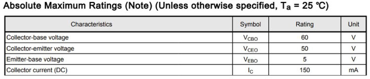
切勿向基极端子施加超过绝对最大额定值表(表1)中所示的发射极-基极额定电压(VEBO)的电压(对于npn晶体管为负偏压,对于pnp晶体管为正偏压)。否则会降低hFE和其它参数。
双极晶体管的发射极浓度最高,其次是基极,然后是集电极。发射极的浓度比基极的浓度高100倍以上。浓度越高,耐电压越低。
VEBO只有几伏。将大幅值信号输入基极时必须小心。此外,有些电路中还施加了反向偏压,例如下面的电路。设计时请考虑使用条件。
当单稳态多谐振荡器由双极晶体管组成时,可向基极施加超过额定VEBO的偏置电压。
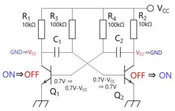
下文介绍了图1中所示的多谐振荡器的操作。
- 假设Q1最初为导通状态。因此,Q1的集电极电压接近GND电平。C1通过R3充电,而C2通过R2充电。
- C1充电后,Q2的基极-集电极电压达到其导通电压(约0.7V),从而导通。Q2的集电极电压降至接近GND的电平。在此之前,C2两端的电压充电至VCC–0.7V。即使Q2的集电极电压下降,C2仍保持充电状态。因此,C2基极端上Q1端子的电压降至0.7V-VCC。重复这些步骤以充当单稳态多谐振荡器。假设VCC=10V,则Q1和Q2的发射极-基极电压达到-9.3V,超过-5V的额定VEBO。
相关信息
以下文件还包含相关信息: