- 型号 & 关键词搜索
- 交叉搜索
- 参数搜索
- 库存查询与购买
This webpage doesn't work with Internet Explorer. Please use the latest version of Google Chrome, Microsoft Edge, Mozilla Firefox or Safari.
请输入3个以上字符 Search for multiple part numbers fromhere.
The information presented in this cross reference is based on TOSHIBA's selection criteria and should be treated as a suggestion only. Please carefully review the latest versions of all relevant information on the TOSHIBA products, including without limitation data sheets and validate all operating parameters of the TOSHIBA products to ensure that the suggested TOSHIBA products are truly compatible with your design and application.Please note that this cross reference is based on TOSHIBA's estimate of compatibility with other manufacturers' products, based on other manufacturers' published data, at the time the data was collected.TOSHIBA is not responsible for any incorrect or incomplete information. Information is subject to change at any time without notice.
请输入3个以上字符
双极结型晶体管(BJT)的工作原理——为何微小电流能够控制大电流?(有源区与饱和区解析)
双极结型晶体管(BJT)通常被认为是在有源区中,集电极电流(IC)可以由基极电流(IB)进行控制的器件。然而,这种关系并不意味着基极电流直接决定集电极电流。实际上,这种电流控制关系是由晶体管内部载流子(电子与空穴)的输运过程所建立的。当载流子输运条件发生变化时,基极电流与集电极电流之间的比例关系将不再成立。因此,晶体管不再作为放大器工作,而是表现为开关器件。
因此,对于BJT的工作机理,不应仅将其理解为简单的“电流控制电流”关系,而应将其视为由器件内部载流子输运条件所支配的一种物理现象。
在本文中,我们将重点探讨载流子传输过程,例如扩散、提取(移除)、存储和复合,并解释活性区与饱和区在工作原理上的差异。
具体来说,本节将涵盖以下内容:
学习要点
- 为什么在有源区中,集电极电流与基极电流成正比
- 为什么这种比例关系在饱和区会失效,以及电流增益(hFE)失去意义的原因
- 为什么饱和区被视为开关器件的导通(ON)状态
本文通过将载流子输运过程与外部电路条件相结合,对上述各项内容进行说明。
为简化说明,本文以NPN型晶体管为对象进行讲解。对于PNP型晶体管,只需对极性进行反转,其工作原理同样适用。
1.双极结型晶体管(BJT)概述
双极结型晶体管(BJT)是一种半导体器件:当基极—发射极结处于正向偏置,且集电极电位高于发射极时,器件内部开始有电流流动。此时,集电极电流会随基极电流的变化而变化。这种状态称为导通状态(ON状态)。
导通状态(ON状态)根据工作条件的不同,可分为有源区和饱和区。相对地,当没有电流流动时,器件处于关断状态(OFF状态),称为截止区。
有源区
在有源区中,基极—发射极结处于正向偏置,集电极—基极结处于反向偏置。在这种条件下,集电极电流随基极电流近似成比例变化。
因此,电流增益hFE较高且基本保持恒定,晶体管在该区域作为电流放大器工作。
饱和区
当外部电路将集电极电压(VCE)充分拉低时,集电极—基极结也会变为正向偏置,晶体管进入饱和区。
在该状态下,有源区中所观察到的基极电流与集电极电流之间的比例关系被破坏。表观电流增益hFE会下降,并且不再适合作为衡量电流控制能力的指标。
因此,晶体管不再作为放大器工作,而是作为处于“导通”(ON)状态的开关器件。
截止区
在截止区中,基极—发射极结未处于正向偏置,因此几乎没有基极电流流动。结果,集电极电流也接近为零。
这种状态称为关断状态(OFF状态)。
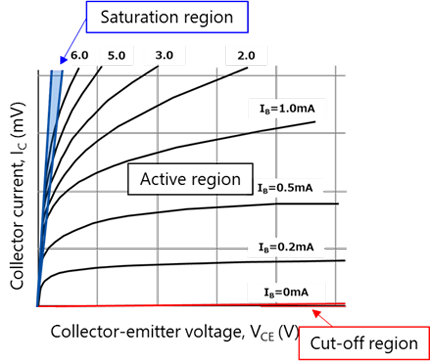
图1:双极结型晶体管的工作区域(有源区、饱和区、截止区)
2.有源区中的电流放大机制
在有源区中,基极—发射极(B–E)结处于正向偏置,基极—集电极(B–C)结处于反向偏置。在这种条件下,电子从发射极注入到基区。
由于基极—发射极(B–E)结处于正向偏置,基区靠近发射极一侧的电子浓度较高。另一方面,由于基极—集电极(B–C)结处于反向偏置,电子会被耗尽区中的电场迅速抽取,使得靠近集电极一侧的电子浓度保持较低水平。
因此,在基区内部形成了电子浓度梯度。该浓度梯度驱动扩散过程,使电子向集电极方向传输。当电子到达耗尽区后,会立即受到电场加速,并被高效地收集到集电极中。
由此,电流放大是通过以下一系列过程实现的:
注入→扩散传输→收集
2-1.基极—发射极正向偏置下的电子注入(输入条件:增加np(0))
在有源区中,基极—发射极结处于正向偏置,从而降低了结区的能量势垒。由此,更多电子能够从发射极跨越势垒进入基区,增加了注入到基区的电子数量,并提高了结边界处的少数载流子电子浓度 np(0)。
通过这种方式,在基区靠近发射极一侧维持了较高的电子浓度。这一条件构成了扩散过程的起始点,并作为决定后续载流子输运的输入边界条件,起着至关重要的作用。
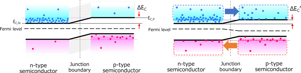
a)未加偏置
b)正向偏置
图2:pn结在零偏置与正向偏置条件下的能带结构图
图2显示了pn结在零偏置和正向偏置条件下的能带结构。
当施加正向偏置时,结处的有效势垒高度降低。由此,能够从n型半导体跨越势垒进入p型半导体的电子数量增加。随着进入p区的电子供给增加,结边界处的少数载流子电子浓度 np(0) 也随之提高。
在双极结型晶体管(BJT)的语境中,这对应于由于正向偏置作用,基区发射极一侧的少数载流子电子浓度增加,即输入边界条件的提升。
补充:结边界处的少数载流子浓度
设np0为无偏置条件下p型区域中的少数载流子电子浓度。当施加正向偏置电压VBE 时,结边界处的电子浓度可表示为:
np(0)=np0 exp(qVBE/kT)
2-2.基区中的扩散传输与B–C结处的收集(输出条件:维持低浓度)
注入到基区中的电子通过扩散在基区内移动。在有源区中,B–C结处于反向偏置状态,从而形成一个电场方向指向集电极的耗尽区。
当在基区中扩散的电子到达耗尽区边缘时,会立即受到电场的加速,并被高效地扫入集电极中(即通过漂移实现收集)。
由于集电极侧的电子被持续移除,因此该处的电子浓度始终保持较低水平(固定的输出条件)。因此,从发射极一侧(高浓度)到集电极一侧(低浓度)形成并维持了浓度梯度,在这一梯度的作用下,扩散传输得以持续稳定地进行。
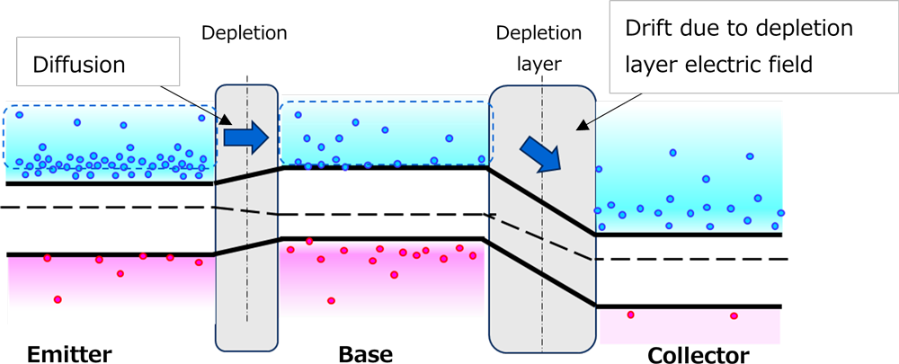
图3:有源区中NPN晶体管的能带示例图
图3显示了NPN晶体管在有源区的能带分布情况。
在发射极与基极之间,载流子在浓度梯度的驱动下通过扩散进行传输;而在基极与集电极之间,电子受到耗尽区内电场的作用,被扫入集电极中(即实现收集过程)。
2-3.基区中的载流子损失与注入不对称性
- 复合导致的损失
由于基区为p型半导体,其中多数载流子为空穴,因此一部分从发射极注入的电子会在基区内与空穴发生复合。
尽管基极电流由多个分量组成,但其主要部分对应该基区内因复合而损失的电子所形成的电流。 - 注入不对称性
在NPN型BJT中,发射极为重掺杂n型,而基区为轻掺杂p型。
由于这种掺杂上的不对称性,当B–E结处于正向偏置时,从发射极向基区的电子注入占主导,而从基区向发射极的空穴注入则被显著抑制。 - 基区中的浓度梯度
在发射极一侧,np(0)较高;而在集电极一侧,电子被耗尽区中的电场迅速抽取,使其浓度保持在较低水平。
因此,在基区内建立起从发射极侧(高浓度)到集电极侧(低浓度)的单向浓度梯度。该梯度驱动扩散电流,从而实现载流子的持续传输。
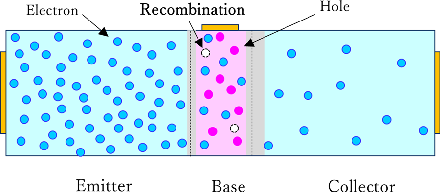
图4:有源区中基区内载流子行为(复合与收集)
图4显示了有源区中基区内电子载流子的行为(包括复合与收集过程)。一部分从发射极注入的电子在基区内发生复合而损失,其余电子则在B–C结处被扫出,并被集电极收集。
2-4.基极电流、集电极电流与hFE之间的关系
在有源区中:
- 由于复合导致的电子损失对应于基极电流IB
- 被收集的电子对应于集电极电流IC
只要维持有源区的工作条件(即输入与输出边界条件),在基区内因复合而损失的载流子比例以及被集电极收集的载流子比例基本保持不变。因此,当注入的载流子数量增加时,复合损失(IB)和被收集的载流子数量(IC)都会按比例随之增加。这正是IC随IB成比例变化的物理原因。
这种比例关系可用直流电流增益hFE表示,其定义为:
hFE=IC/IB
因此,hFE并不是源于某种额外的“放大机制”,而是由载流子输运过程——“注入、复合与收集”——所表现出来的结果。
2-5.有源区本章总结
在有源区中,B–E结处于正向偏置,提高了输入边界条件np(0);同时,B–C结处于反向偏置,使输出边界条件保持在较低水平。这些输入与输出条件在基区内建立起浓度梯度。电子在该梯度的驱动下通过扩散进行传输,并在耗尽区电场作用下被高效地收集。
同时,基区内会发生复合损失,这表现为基极电流IB。只要工作条件保持不变,损失比例就不会发生显著变化,因此IB和IC都会随注入载流子数量按比例增加,且在有源区内hFE始终可以作为有效的电流增益。
3.为何在饱和区中电流放大不再成立(内部条件的失效)
在饱和区中,B–E结和B–C结均处于正向偏置状态。
这改变了集电极侧的边界条件:电子浓度不再保持在较低水平,而是上升。因此,基区内的浓度梯度减小。
由于该梯度减弱,扩散传输变得不再高效。电子在基区中的停留时间延长,从而导致复合增加。
其结果是,到达集电极的电子比例下降,集电极电流不再随基极电流成比例增加。
3-1.向饱和区过渡:
边界条件的变化(输出条件)
饱和区对应于这样一种状态:基极—发射极结仍保持正向偏置,而随着集电极电压VCE的降低,基极—集电极结也转为正向偏置。
在这种条件下,在有源区中成立的“基极—集电极结必须处于反向偏置”的要求已不再满足。
其结果是,基区靠近集电极一侧的电子浓度(即输出边界条件)不再保持在较低水平,而是发生升高,从而改变了控制载流子输运的条件。
3-2.边界条件的变化及其引起的浓度分布变化
(浓度梯度的减小)
在有源区中,基极—集电极结处于反向偏置。因此,集电极侧的电子浓度保持在较低水平,从而在发射极一侧与集电极一侧之间建立起较大的浓度差。由此,在基区内形成了从发射极侧指向集电极侧的清晰电子浓度梯度。相比之下,在饱和区中,基极—集电极结同样处于正向偏置状态。从能带结构的角度来看(见图6),此时的载流子输运条件已不同于有源区。在有源区中,电子在基极—集电极结耗尽区电场的作用下被扫向集电极;而在饱和区中,该电场减弱,同时会有少量电子从集电极向基区注入。虽然这种来自集电极的注入远小于来自发射极的注入,但仍会提高集电极侧的电子浓度,从而减小其与发射极侧之间的浓度差。因此,在基区内形成的浓度梯度变得更加平缓,基于该梯度的扩散驱动力随之减弱。在有源区中,由于存在较大的浓度梯度,能够实现高效的扩散传输;而在饱和区中,浓度梯度减小,导致电子扩散传输效率下降。这种浓度分布的变化如图5所示。从能带结构的角度(见图6)也可以对载流子输运条件的变化进行理解。
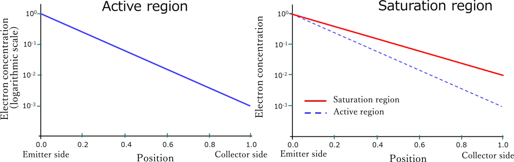
图5:有源区与饱和区基区内电子浓度分布(对数坐标)
图5比较了有源区与饱和区在基区内的电子浓度分布(对数坐标)。在有源区中,集电极一侧的电子浓度保持较低,因此在基区形成较大的浓度梯度(dn/dx)而在饱和区中,集电极一侧的电子浓度上升,从而减小了浓度差,使浓度梯度变得更加平缓。饱和区图中的虚线表示用于对比的有源区浓度分布。纵轴表示经过归一化处理的对数相对值,其中发射极侧边界处的电子浓度np(0),被设定为1(=10^0)。
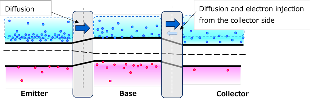
图6:NPN晶体管在饱和区的能带图
图6显示了NPN晶体管在饱和区时的能带结构。在发射极与基极之间,载流子的传输仍然以扩散为主,这与有源区时的情况相同。相比之下,基极–集电极结处于正向偏置,这会降低结两端的电势差,并削弱耗尽区中的电场。因此,基极与集电极之间的电子传输也主要由扩散过程主导。此外,还存在少量电子从集电极(在该区域电子为多数载流子)注入到基极中的现象。
3-3.由于浓度梯度的降低,载流子驻留时间和复合率增加
即使在饱和区,只要基极–发射极结仍然保持正向偏置,来自发射极的电子注入就会持续进行。然而,正如前一节所述,浓度梯度的降低会导致基区内电子的扩散传输速率下降。
因此,电子载流子会在基区中停留更长时间。
随着驻留时间的增加,电子在基区中停留的时间更长,更容易与基区中的空穴发生复合。因此,由复合而损失的电子载流子比例增加。能够到达集电极的电子载流子比例随之减少,即使增大基极电流,集电极电流也不再像在有源区那样成比例增加。
3-4.从电路角度的行为:
hFE的意义丧失及向开关导通状态的转变
在饱和区,增加基极电流已不再导致集电极电流成比例增加。这种现象也可以从电路角度来理解。
在该区域中,由于负载等外部电路条件的影响,集电极电压会下降,晶体管的工作点是在这种电压约束下确定的。因此,集电极电流主要受到外部电路的限制,而不再由基极电流来控制。
因此,尽管这个比值
hFE=IC/IB
仍然可以计算出来,但它已不再具有作为电流控制指标的实际意义。这是因为在这种条件下,集电极电流不再由基极电流所主导。
因此,在饱和区,晶体管不再作为电流放大器工作,而是作为处于导通状态(ON状态)的开关来运行。
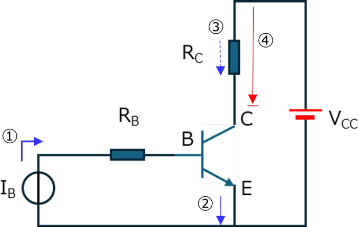
图7:饱和区中的共射极电路及其与载流子传输的关系
图7显示了工作在饱和区的共射极电路以及相应的内部载流子传输状态。图中用①到④标示的顺序说明了如下过程.
随着基极电流IB的增加,发射极电流IE也相应增加。这会使通过外部负载的集电极电流IC增大。然而,集电极电流的增加会导致负载电阻上的电压降增大,从而使集电极电压VC(即VCE)降低。
随着VCE的降低,基极–集电极结逐渐接近正向偏置,基区内的载流子传输条件开始发生变化。具体而言,电子的浓度梯度减小,这会增加载流子在基区中的驻留时间,并增强复合现象。
因此,集电极电流不再随着基极电流成比例增加,晶体管进入饱和区。
3-5. 饱和区总结
在饱和区中,基极–集电极结的正向偏置会改变输出端的边界条件,并使集电极一侧的电子浓度增加,从而导致基区内的浓度梯度减小。
因此,电子的扩散传输效率降低,载流子在基区中的驻留时间增加,复合损失也变得更加显著。
因此,集电极电流不再随着基极电流成比例增加,而电流增益hFE也不再具有作为电流控制指标的意义。
在这种条件下,晶体管不再作为电流放大器工作,而是作为处于导通状态(ON状态)的开关来发挥作用。
对于双极结型晶体管(BJT)所使用的“饱和区”这一术语,其物理含义与MOSFET中使用的同一术语有着显著的不同。
在双极结型晶体管(BJT)中,饱和区指的是电流放大作用不再成立、器件转而作为开关使用的一种工作状态。相比之下,在MOSFET中,饱和区只是沟道已经形成的一种正常工作区间,并不意味着电流放大功能的失效,也不直接等同于开关行为本身。
有关MOSFET工作区域(截止区、线性区和饱和区)及其物理意义的详细说明,请参阅以下常见问题(FAQ):
理解MOSFET的工作原理与机制|截止区、线性区和饱和区详解
相关信息
以下文档也包含相关信息: