- 型号 & 关键词搜索
- 交叉搜索
- 参数搜索
- 库存查询与购买
This webpage doesn't work with Internet Explorer. Please use the latest version of Google Chrome, Microsoft Edge, Mozilla Firefox or Safari.
请输入3个以上字符 Search for multiple part numbers fromhere.
The information presented in this cross reference is based on TOSHIBA's selection criteria and should be treated as a suggestion only. Please carefully review the latest versions of all relevant information on the TOSHIBA products, including without limitation data sheets and validate all operating parameters of the TOSHIBA products to ensure that the suggested TOSHIBA products are truly compatible with your design and application.Please note that this cross reference is based on TOSHIBA's estimate of compatibility with other manufacturers' products, based on other manufacturers' published data, at the time the data was collected.TOSHIBA is not responsible for any incorrect or incomplete information. Information is subject to change at any time without notice.
请输入3个以上字符
双极结型晶体管(BJT)的集电极端和发射极端能否互换?
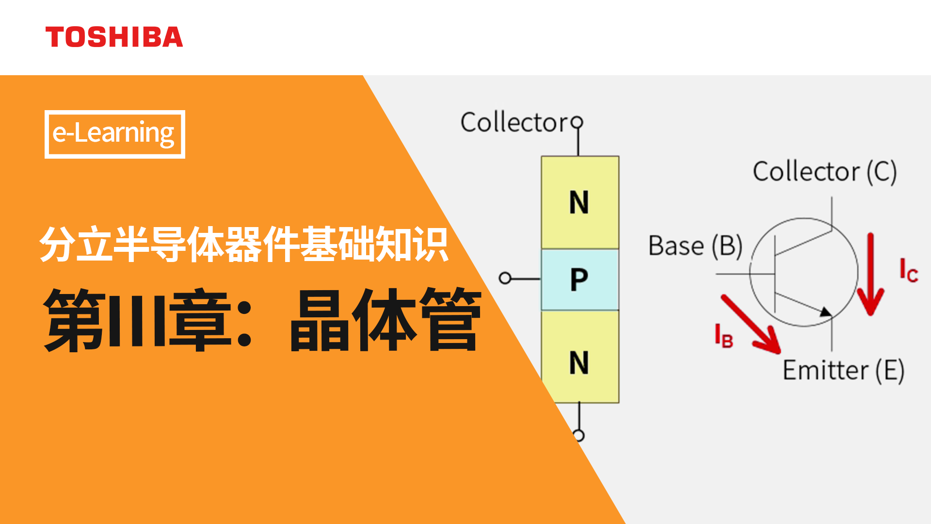
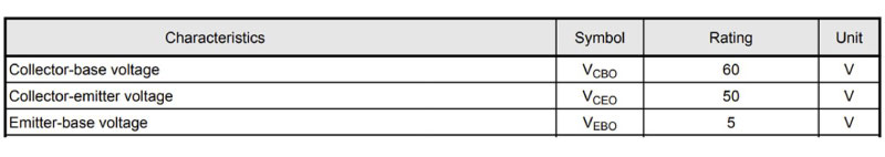
双极结型晶体管(BJT)的设计为在正确连接时提供最佳性能。当反向连接时,其性能较差(低 hFE)。然而,能够施加到集电极-基极电压的电压非常低。该电压不能超过绝对最大额定值(VEBO)(表1)。互换集电极和发射极端不仅会降低晶体管性能,还可能对器件造成永久性损坏。
通常,双极晶体管的设计需保证实现高hFE。为实现此目的,发射极中的大量载流子(在npn晶体管中为电子)必须扩散至基极区,然后有效地穿过基极区进入集电极。还必须控制集电极区中的耗尽层,以增强晶体管的耐受电压(即集电极-基极电压,VCBO)。可通过以下方式满足这些条件:
- 使发射极区中的掺杂浓度高于基极区中的掺杂浓度;
- 减小基极区的厚度;
- 降低集电极区中的掺杂浓度。
因此,三个半导体区域中的掺杂浓度具有以下关系:发射极>>基极>集电极。
普通晶体管由于集电极浓度低而保持高击穿电压(VCBO/VCEO)。 如果反向连接,高浓度发射极将充当集电极,能够施加的电压(VEBO)将变得极低。
如果集电极端子和发射极端子反向连接,则不满足上述关系。在这种情况下,hFE会降低,从而使双极晶体管无法按预期工作,并可能导致基极电流超过其规定的额定值。此外,由于VCEO降低,晶体管关断时可能会击穿。由于上述原因,反向连接的晶体管可能会永久损坏。
除了设计为反向连接的静音晶体管*外,必须按正常方向连接典型的双极晶体管。
*目前,东芝不提供静音晶体管。
相关信息
以下文件还包含相关信息: