- 型号 & 关键词搜索
- 交叉搜索
- 参数搜索
- 库存查询与购买
This webpage doesn't work with Internet Explorer. Please use the latest version of Google Chrome, Microsoft Edge, Mozilla Firefox or Safari.
请输入3个以上字符 Search for multiple part numbers fromhere.
The information presented in this cross reference is based on TOSHIBA's selection criteria and should be treated as a suggestion only. Please carefully review the latest versions of all relevant information on the TOSHIBA products, including without limitation data sheets and validate all operating parameters of the TOSHIBA products to ensure that the suggested TOSHIBA products are truly compatible with your design and application.Please note that this cross reference is based on TOSHIBA's estimate of compatibility with other manufacturers' products, based on other manufacturers' published data, at the time the data was collected.TOSHIBA is not responsible for any incorrect or incomplete information. Information is subject to change at any time without notice.
请输入3个以上字符
当偏置电阻内置晶体管(BRT)导通时获得必要的电压(即降低“导通”状态下集电极-发射极电压降)
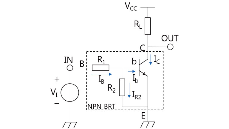
图1显示了使用NPN BRT的基本开关电路。
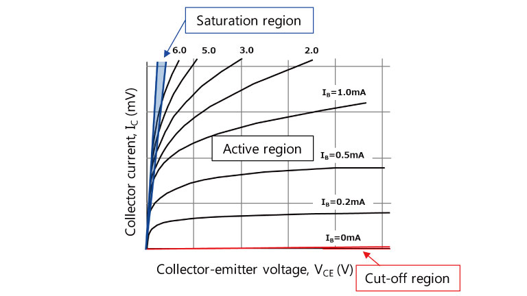
当NPN BRT在饱和区导通时,由于外部电阻(RL)和集电极电流(IC),其集电极电压降至GND电平。但是,实际上,集电极和GND(发射极)电位之间有一个称为集电极-发射极饱和电压(VCE(sat))的电压电平。可通过增加基极电流(IB)来降低VCE(sat)。
(由于当图1的电路处于“导通”状态时,VCE(sat) << VCC,故IC = VCC/RL,这几乎恒定不变。因此,增加IB会导致hFE(= IC/IB)减小。这意味着BRT达到更深的饱和度,从而降低了VCE(sat)。)
通常,只能将有限范围的电压施加至基极。因此,让我们考虑如何在特定的基极电压下使更多的基极电流(Ib)。
内部基极电流(Ib)表示如下:
Ib=IB–IR2=(VI–Vbe)/R1–Vbe/R2
其中,VI为输入电压,Vbe为内部晶体管的基极-发射极电压,可以将其视为恒定在大约0.7V*。
Ib等式表明可通过使用BRT来增加Ib:
1)R1小值
2)R2大值
这并不意味着电阻比(R1/R2)较小的BRT,而是R1值较小的BRT。这种BRT在特定输入电压(VI)下会向基极传输更大的电流。
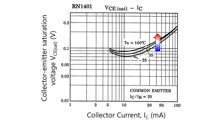
但这种BRT的缺点是其会消耗更多的功率并进入更深的饱和度的状态,从而导致开关速度降低。同样,饱和电压随着温度的升高而增加,如图4所示。
需考虑这些因素以实现最佳设计。
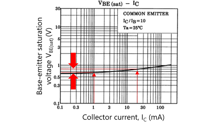
*:图3显示了通用型2SC2712晶体管的VBE(sat)–IC曲线,该晶体管相当于BRT中使用的晶体管。在使用BRT的IC范围内,VBE的变化仅为数百毫伏。VBE的这种变化相对于输入电压可忽略不计。