- 型号 & 关键词搜索
- 交叉搜索
- 参数搜索
- 库存查询与购买
This webpage doesn't work with Internet Explorer. Please use the latest version of Google Chrome, Microsoft Edge, Mozilla Firefox or Safari.
请输入3个以上字符 Search for multiple part numbers fromhere.
The information presented in this cross reference is based on TOSHIBA's selection criteria and should be treated as a suggestion only. Please carefully review the latest versions of all relevant information on the TOSHIBA products, including without limitation data sheets and validate all operating parameters of the TOSHIBA products to ensure that the suggested TOSHIBA products are truly compatible with your design and application.Please note that this cross reference is based on TOSHIBA's estimate of compatibility with other manufacturers' products, based on other manufacturers' published data, at the time the data was collected.TOSHIBA is not responsible for any incorrect or incomplete information. Information is subject to change at any time without notice.
请输入3个以上字符
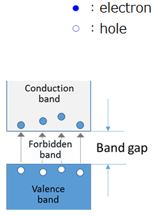
什么是宽带隙半导体?

电子和空穴从价带跃迁至导带所需的能量即称为带隙。硅(Si)的带隙为1.12eV(电子伏特)。具有较大值的半导体即称为宽带隙半导体。碳化硅(SiC)和氮化镓(GaN)都是宽带隙半导体。
典型半导体材料的物理特性常数如下表所示。
由于宽带隙半导体的晶格常数较小,因此原子之间的键合强度变强。这意味着高介电击穿强度和导热系数。
4H-SiC的带隙为3.26eV,介电击穿强度为2.8×10⁶,与Si的3×10⁵相比,这是一个非常大的值。
Si和主要宽带隙半导体的物理特性常数
| 特性 | 单位 | Si | 4H-SiC | 6H-SiC | 3C-SiC | GaN | GaAs | 金刚石 |
|---|---|---|---|---|---|---|---|---|
| 带隙 | eV | 1.12 | 3.26 | 3.02 | 2.23 | 3.39 | 1.43 | 5.47 |
| 电子迁移率μe | cm2/Vs | 1400 | 1000/1200 | 450/100 | 1000 | 900 | 8500 | 2200 |
| 空穴迁移率μh | 600 | 120 | 100 | 50 | 150 | 400 | 1600 | |
| 介电击穿强度Ec | V/cm | 3.0×10⁵ | 2.8×10⁶ | 3.0×10⁶ | 1.5×10⁶ | 3.3×10⁶ | 4.0×10⁵ | 1.0×10⁷ |
| 导热系数λ | W/cmK | 1.5 | 4.9 | 4.9 | 4.9 | 2.0 | 0.5 | 20 |
| 饱和电子漂移速度Vsat | cm/s | 1.0×10⁷ | 2.2×10⁷ | 1.9×10⁷ | 2.7×10⁷ | 2.7x10⁷ | 2.0×10⁷ | 2.7×10⁷ |
| 相对介电常数ε | 11.8 | 9.7/10.2 | 9.7/10.2 | 9.7 | 9.0 | 12.8 | 5.5 |

