- 型号 & 关键词搜索
- 交叉搜索
- 参数搜索
- 库存查询与购买
This webpage doesn't work with Internet Explorer. Please use the latest version of Google Chrome, Microsoft Edge, Mozilla Firefox or Safari.
请输入3个以上字符 Search for multiple part numbers fromhere.
The information presented in this cross reference is based on TOSHIBA's selection criteria and should be treated as a suggestion only. Please carefully review the latest versions of all relevant information on the TOSHIBA products, including without limitation data sheets and validate all operating parameters of the TOSHIBA products to ensure that the suggested TOSHIBA products are truly compatible with your design and application.Please note that this cross reference is based on TOSHIBA's estimate of compatibility with other manufacturers' products, based on other manufacturers' published data, at the time the data was collected.TOSHIBA is not responsible for any incorrect or incomplete information. Information is subject to change at any time without notice.
请输入3个以上字符
5、TVS二极管 (ESD保护二极管) 的布局注意事项
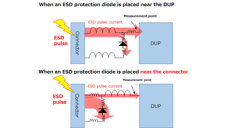
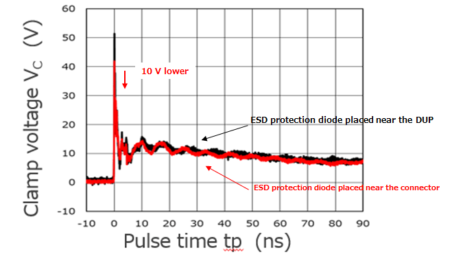
注意,ESD保护二极管位置影响ESD保护性能。
1.ESD保护二极管靠近ESD进入点。
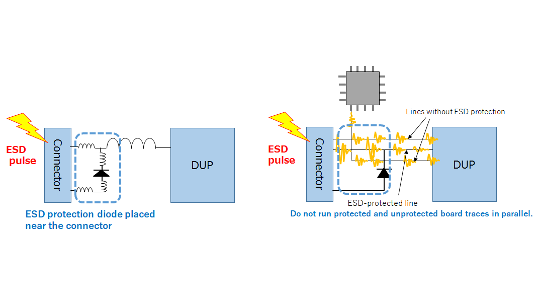
2.在来自连接器的电路板走线分支成ESD保护二极管和DUP的两条线路后,使与ESD 保护二极管(包括GND)串联的走线电感降至最低。


3.不要将任何电路板走线与可能引入ESD脉冲的信号走线并行。特别是,避免ESD抗扰度低的器件电路板走线与可能受ESD事件影响的电路板走线并行。
- 1/1
相关信息
- 产品页
TVS二极管(ESD保护二极管) - 应用说明
二极管 - FAQ
TVS二极管(ESD保护二极管) - 查看所有东芝 TVS 二极管(ESD 保护二极管)产品的参数:
参数搜索 - 查询TVS二极管(ESD保护二极管)的库存并购买:
库存查询与购买

