


- 型号 & 关键词搜索
- 交叉搜索
- 参数搜索
- 库存查询与购买
This webpage doesn't work with Internet Explorer. Please use the latest version of Google Chrome, Microsoft Edge, Mozilla Firefox or Safari.
请输入3个以上字符 Search for multiple part numbers fromhere.
The information presented in this cross reference is based on TOSHIBA's selection criteria and should be treated as a suggestion only. Please carefully review the latest versions of all relevant information on the TOSHIBA products, including without limitation data sheets and validate all operating parameters of the TOSHIBA products to ensure that the suggested TOSHIBA products are truly compatible with your design and application.Please note that this cross reference is based on TOSHIBA's estimate of compatibility with other manufacturers' products, based on other manufacturers' published data, at the time the data was collected.TOSHIBA is not responsible for any incorrect or incomplete information. Information is subject to change at any time without notice.
请输入3个以上字符
低开关损耗SiC肖特基二极管(SBD)
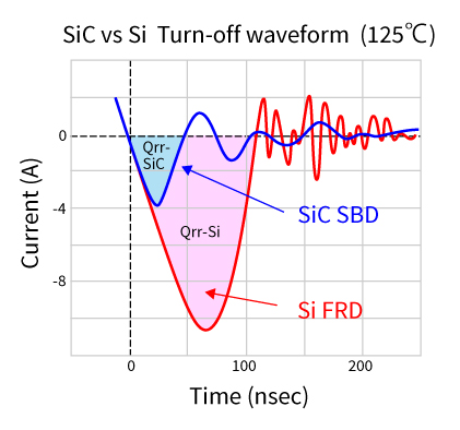
SBD是由半导体与金属的接合形成的单极器件。原则上,SBD没有反向恢复时间,不像使用pn结二极管会引起问题。因此,SBD有助于大幅度降低关断时的开关损耗。
因为传导是由空穴和电子引起的,所以pn结二极管是双极的。pn结二极管具有反向恢复时间,因为在关断期间少数载流子(p层中的电子和n层中的空穴)会保留在结处。相反,单极的SBD没有反向恢复时间。但由于金属和半导体接合处的耗尽区具有电容,因此其充电和放电将产生电流流动。虽然该电容是温度和反向偏压的函数,但在典型的SiC SBD应用所工作的高压区几乎不受影响。
此外,该电容不是电流的函数。与pn结二极管的电容不同,当电流小于额定直流电流时,它几乎不依赖于电流。但是具有MPS结构的SiC SBD在电流超过额定直流值时可能会受到少数载流子的影响。
SBD的电容计算如下:
C(VR)=S x [ ε×q×Nd/{2×(Vbi+VR)}]^0.5
Vbi:内置电压(=金属的功函数—n型(p型)半导体的功函数)
S:结区,ε:介电常数,q:单位电荷,Nd:掺杂浓度
VR:反向偏置电压
虽然Vbi是温度的函数,因为Vbi << VR,所以可忽略。
SiC肖特基二极管
仿真器
相关信息
购买、样品、及IC可靠性查询
库存查询与购买
请输入3个以上字符
Through this website you are able to proceed to the website of our distributors ("Third Party Website") which is not under the control of Toshiba Corporation and its subsidiaries and affiliates (collectively "Toshiba"). The Third Party Website is made available to you as a convenience only and you agree to use the Third Party Website at your own risk. The link of the Third Party Website does not necessarily imply a recommendation or an endorsement by Toshiba of the Third Party Website. Please be aware that Toshiba is not responsible for any transaction done through the Third Party Website, and such transactions shall be subject to terms and conditions which may be provided in the Third Party Website.