


- 型号 & 关键词搜索
- 交叉搜索
- 参数搜索
- 库存查询与购买
This webpage doesn't work with Internet Explorer. Please use the latest version of Google Chrome, Microsoft Edge, Mozilla Firefox or Safari.
请输入3个以上字符 Search for multiple part numbers fromhere.
The information presented in this cross reference is based on TOSHIBA's selection criteria and should be treated as a suggestion only. Please carefully review the latest versions of all relevant information on the TOSHIBA products, including without limitation data sheets and validate all operating parameters of the TOSHIBA products to ensure that the suggested TOSHIBA products are truly compatible with your design and application.Please note that this cross reference is based on TOSHIBA's estimate of compatibility with other manufacturers' products, based on other manufacturers' published data, at the time the data was collected.TOSHIBA is not responsible for any incorrect or incomplete information. Information is subject to change at any time without notice.
请输入3个以上字符
改进JBS结构以降低泄漏电流和提高浪涌电流能力: SiC肖特基势垒二极管 (SiC SBD)
肖特基二极管(SBD)具有反向恢复时间(trr)短、正向电压(VF)低等优点,但也存在泄漏电流大等缺点。东芝的SiC SBD使用改进的结构克服了这个缺点。
JBS结构降低泄漏电流(IR)
SBD是由半导体与金属的接合形成的。由于半导体和金属之间的势垒不同,它起着二极管的作用。由于半导体-金属界面上的分子结构可能是不连续的,因此可能会出现表面不规则、晶体缺陷或其它异常现象。当强电场作用于含有这些缺陷的半导体-金属界面时,会有所谓的泄漏电流(IR)流动。
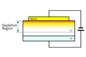
在具有传统结构的SBD中,耗尽区延伸到半导体侧(如下所示),导致电荷(或电子)产生的电场在半导体-金属界面处最强。
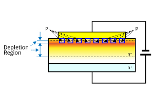
相反,在JBS二极管中,耗尽区延伸于部分埋在半导体表面下的p和n-区之间。当反向偏压增大时,p型耗尽区相互穿插,最大电场位置直接移动到p区下面。这会减少可能存在缺陷的表面上的电场,从而减少泄漏电流。
集成PiN肖特基(MPS)结构提高浪涌电流能力
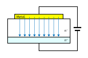
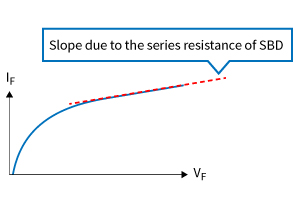
当传统的SBD正向偏置时,电流流过以下路径:金属 → 肖特基势垒 → Si (n-) → Si(n+)。由于掺杂浓度较低,Si(n-)层电阻较大。因此,此SBD的IF-VF曲线如下所示。
SiC SBD的应用包括PFC电路,PFC电路必须保证在大电流下工作,因为它们在电源接通和负载变化时都会瞬间暴露在大电流条件下。在这种情况下,具有如下所示的IF-VF曲线的SBD可能发生过热现象。
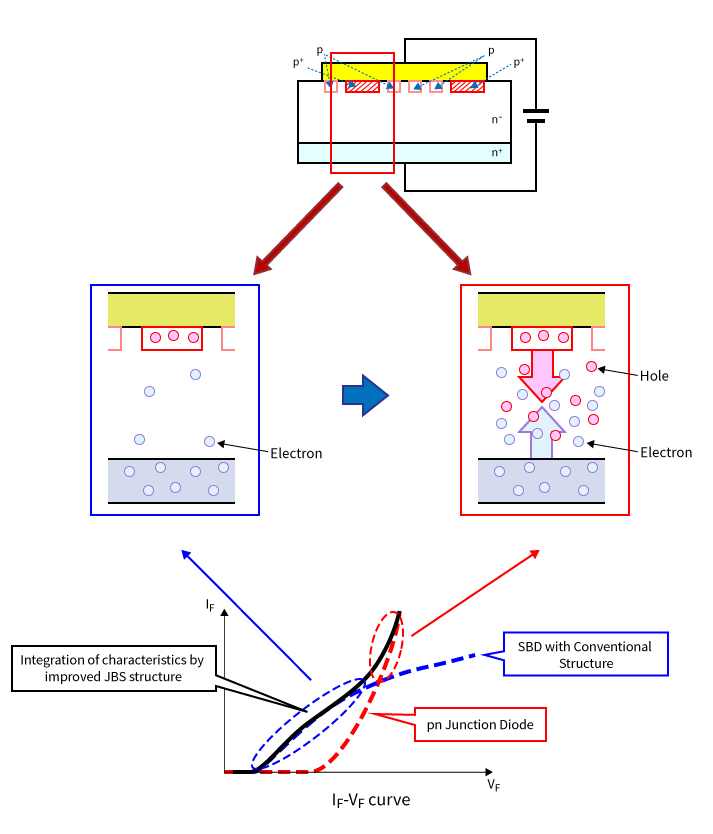
为了解决这个问题,东芝开发了一种新的SBD,它采用改进的JBS结构,其中包含了集成PiN-肖特基(MPS)结构的概念。MPS结构是其p+区埋在SBD的n-区中,如下所示。在东芝的设计中,JBS结构的部分p层(图中阴影部分)被放大,这部分的杂质浓度增加。p+区和n-区形成一个pn结二极管,在需要大电流(浪涌电流)时打开。这增加了SBD的载流能力,因此即使在大电流下也能降低正向电压的升高,并增加最大允许浪涌电流值。
MPS结构的特点是在阳极电极下方的p+–n-–n+结构。
在低电流下,n-区通常具有高电阻。然而,当SBD正向偏压时,空穴和电子分别从p区和n区流入n-区,同时保持电中性。在这个时候,空穴和电子都存在于高浓度的n-区内。因此,n-区将作为高掺杂浓度区域,特别是在高电流下,表现出非常低的电阻(传导性调制)。因此,该SBD具有如下所示的IF-VF曲线,在高电流区域具有低VF。
SiC肖特基二极管
相关信息
购买、样品、及IC可靠性查询
库存查询与购买
请输入3个以上字符
Through this website you are able to proceed to the website of our distributors ("Third Party Website") which is not under the control of Toshiba Corporation and its subsidiaries and affiliates (collectively "Toshiba"). The Third Party Website is made available to you as a convenience only and you agree to use the Third Party Website at your own risk. The link of the Third Party Website does not necessarily imply a recommendation or an endorsement by Toshiba of the Third Party Website. Please be aware that Toshiba is not responsible for any transaction done through the Third Party Website, and such transactions shall be subject to terms and conditions which may be provided in the Third Party Website.