- 型号 & 关键词搜索
- 交叉搜索
- 参数搜索
- 库存查询与购买
This webpage doesn't work with Internet Explorer. Please use the latest version of Google Chrome, Microsoft Edge, Mozilla Firefox or Safari.
请输入3个以上字符 Search for multiple part numbers fromhere.
The information presented in this cross reference is based on TOSHIBA's selection criteria and should be treated as a suggestion only. Please carefully review the latest versions of all relevant information on the TOSHIBA products, including without limitation data sheets and validate all operating parameters of the TOSHIBA products to ensure that the suggested TOSHIBA products are truly compatible with your design and application.Please note that this cross reference is based on TOSHIBA's estimate of compatibility with other manufacturers' products, based on other manufacturers' published data, at the time the data was collected.TOSHIBA is not responsible for any incorrect or incomplete information. Information is subject to change at any time without notice.
请输入3个以上字符
偏置电阻内置晶体管(BRT)的基极可施加的最大电压是多少?(内置电阻的允许功耗是多少瓦?)

对于典型应用(输入电压(VI)低于10V),您无需考虑最大允许基极电压,但是当VI高于10V时,则需格外小心。
最大输入电压(VI)主要取决于以下因素:
1.串联基极电阻(R1)的值(即R1的功耗)
2.最大集电极电流(IC)
最大输入电压因BRT(例如,hFE)使用条件的不同而有所变化,但是如果R1值较小,则该电压通常取决于集电极电流;如果R1值较大,则取决于R1的值。
1. 串联基极电阻(R1)的值与输入电压(VI)之间的关系
BRT的内置电阻的允许功耗为1/8W。假设处于“导通”状态的内部晶体管的基极-发射极电压为Vbe。然后,流过R1(IB)的电流用以下等式表示。为简单起见,设Vbe =0.7V。
IB=(VI – Vbe )/R1 =(VI – 0.7)/R1
由于IB而引起的R1的功耗不得超过1/8W。因此:
1/8 W > R1 * { ( VI – 0.7 ) / R1 }^2
> ( VI – 0.7 ) ^2 / R1
VI < √( R1 / 8 ) + 0.7
2. 最大集电极电流(IC(最大值))和输入电压(VI)之间的关系The 将最大集电极电流(IC(最大值))规定为绝对最大额定值,即使瞬时也不得超过该最大额定值。
由于BRT在饱和区工作,因此其hFE在10-20的范围内。可通过从上面计算的IB值减去流至R2(IR2)的电流来计算流至内部晶体管(Ib)的基极(b)电流:
Ib = IB – IR2 = ( VI – Vbe ) / R1 – Vbe / R2 = ( VI – 0.7 ) / R1 – 0.7 / R2
由于集电极电流(IC)等于Ib乘以hFE,因此必须满足以下等式:
IC (max) > IC = hFE * IB = hFE * {( VI – 0.7 ) / R1 – 0.7 / R2 }
VI < R1 * IC(max) / hFE +( R1 + R2 ) * 0.7 / R2
根据上述两个因素计算得出的VI值中的较小者即为最大允许基极电压。
1. 串联基极电阻值(R1)
VI < √( R1 / 8 ) + 0.7
2. 最大集电极电流(IC(最大值))
VI < R1 * IC (max) / hFE +( R1 + R2 ) * 0.7 / R2
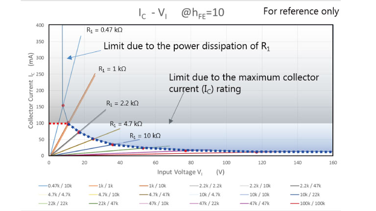
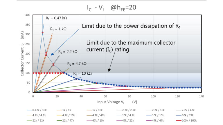
图2和图3显示了在不同电阻值条件下输入电压与集电极电流之间的关系。
尽管最大输入电压及其限制因素取决于BRT的hFE(IC/IB),但以下为正确情况:
- 当R1值较小时:最大输入电压取决于数据表中规定的绝对最大集电极电流。
- 当R1值较大时:最大输入电压取决于R1的功耗。