- 型号 & 关键词搜索
- 交叉搜索
- 参数搜索
- 库存查询与购买
This webpage doesn't work with Internet Explorer. Please use the latest version of Google Chrome, Microsoft Edge, Mozilla Firefox or Safari.
请输入3个以上字符 Search for multiple part numbers fromhere.
The information presented in this cross reference is based on TOSHIBA's selection criteria and should be treated as a suggestion only. Please carefully review the latest versions of all relevant information on the TOSHIBA products, including without limitation data sheets and validate all operating parameters of the TOSHIBA products to ensure that the suggested TOSHIBA products are truly compatible with your design and application.Please note that this cross reference is based on TOSHIBA's estimate of compatibility with other manufacturers' products, based on other manufacturers' published data, at the time the data was collected.TOSHIBA is not responsible for any incorrect or incomplete information. Information is subject to change at any time without notice.
请输入3个以上字符
电阻有哪些变化?

如数据表中所示,串联偏置电阻(R1)的值与数据表中的典型值相差±30%。未单独指定基极-发射极电阻(R2)的值,但指定了电阻比(R1/R2)。R1/R2与典型值相比有±10%的变化。
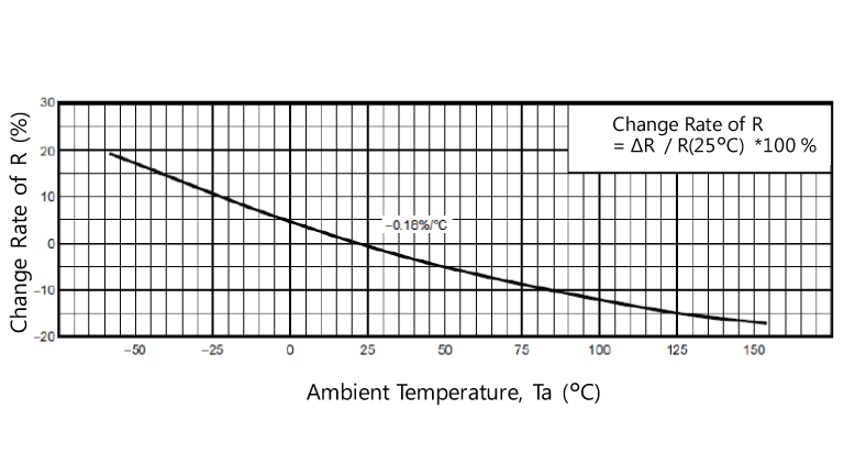
偏置电阻的值取决于温度,如图2所示。电阻以大约0.2%/°C的速率降低。
关于电阻R1:
R1将施加至BRT的B端子的电压转换为电流。双极晶体管是一种电流驱动式器件。当双极晶体管被电压驱动时,集电极电流相对于电压的变化率变大,使得难以控制集电极电流。BRT中的R1使控制集电极电流相对容易一些。当BRT导通时,内部晶体管将在hFE (=IC/Ib)处于10-20范围内的饱和区内工作,具体取决于输入电压。因此,大约几毫安的相对大电流(IB)流经R1。由于R1的允许功耗为1/8W,因此R1值较高的BRT的最大输入电压(VI)由R1值确定。
(详见常见问题(FAQ)“偏置电阻内置晶体管(BRT)的基极可施加的最大电压是多少”。)
关于电阻比(R1/R2)
输入电压(导通)规格(VI(ON))取决于R1/R2。由于基极电流(IB)不会在晶体管导通之前立即流动,因此施加至B端子(VI)的电压会被R1和R2分压。将内部晶体管的导通阈值电压设为Vbe。然后,
Vbe=R2 /(R1+R2)* VI(ON)
如果其包含相同的晶体管,则BRT的Vbe不受R1和R2值的影响。
VI(ON)=Vbe*(R1+R2)/ R2=Vbe*( 1+R1/R2)
因此,VI(ON)取决于电阻比(R1/R2)。


