- 型号 & 关键词搜索
- 交叉搜索
- 参数搜索
- 库存查询与购买
This webpage doesn't work with Internet Explorer. Please use the latest version of Google Chrome, Microsoft Edge, Mozilla Firefox or Safari.
请输入3个以上字符 Search for multiple part numbers fromhere.
The information presented in this cross reference is based on TOSHIBA's selection criteria and should be treated as a suggestion only. Please carefully review the latest versions of all relevant information on the TOSHIBA products, including without limitation data sheets and validate all operating parameters of the TOSHIBA products to ensure that the suggested TOSHIBA products are truly compatible with your design and application.Please note that this cross reference is based on TOSHIBA's estimate of compatibility with other manufacturers' products, based on other manufacturers' published data, at the time the data was collected.TOSHIBA is not responsible for any incorrect or incomplete information. Information is subject to change at any time without notice.
请输入3个以上字符
偏置电阻内置晶体管(BRT)的导通电压和关断电压分别是多少?
数据表中的导通阈值和关断阈值分别被定义为“输入电压(导通)”(VIN(ON))和“输入电压(关断)”(VIN(OFF))。
- 输入电压(导通),VIN(ON):在Ta=25°C时获得等于或高于规定值(例如,IC≥5mA)的集电极电流所需的电压
- 输入电压(关断),VIN(OFF):在Ta = 25°C时使集电极电流低于规定值(例如,IC≤0.1 mA)所需的电压
我们来考虑一下NPN BRT导通的情况。
当NPN BRT关断时,其内部晶体管Q不工作。因此,施加至B端子的输入电压(VI)被R1和R2分压,然后被施加至Q的基极(b)。随着VI的增加,基极-发射极(be)电压(Vbe)超过阈值(典型值:0.7V),Q导通。输入电压(导通)是指为提供5mA或更大的集电极电流所需的电压,但概念相同。
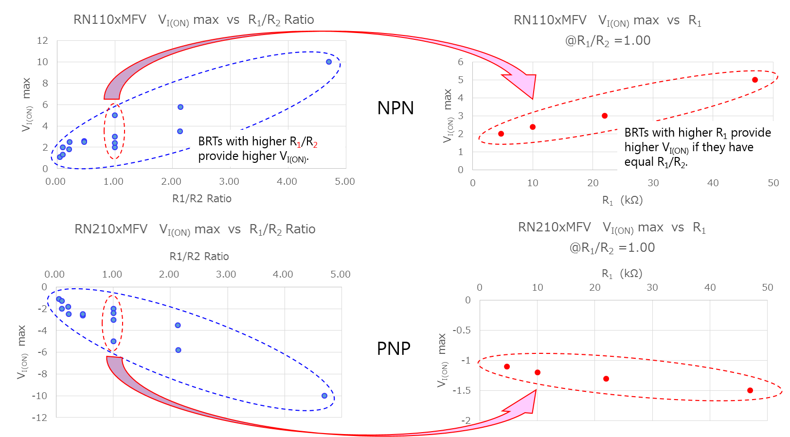
因此,电阻比(R1/R2)较小的BRT在较低的输入电压(VIN(ON))时达到阈值电压。但是,如果电阻比相等,R1值较大的BRT的IB较低。
例如,将提供5mA集电极电流所需的输入电压设为VI1。然后,无论内置电阻如何,内置晶体管的基极电流ib和b-e电压Vbe分别在ib1和Vbe1条件下保持恒定。使用这些变量,Vin可用下列等式表示:
Vin1 = R1 * Ib1 + ( 1 + R1 / R2 ) * Vbe
在特定的阻值比下,仅右侧的第一项“R1*Ib”有变化。因此,可认为Vin1随着R1的增加而增加。(详见图3)
同理,电阻比较低的BRT的输入电压(关断)也较低。但是,相较于电阻比和输入电压(导通)之间的关系,电阻比和输入电压(关断)之间关系的不那么明显,因为输入电压(关断)的测试条件低至0.1mA,因此往往会受器件变化的影响。
尽管PNP BRT的数字符号与NPN BRT的数字符号相反,但以上讨论也适用于PNP BRT。
图2的IC – VI(ON)曲线表明,在特定的输入电压下,集电极电流骤变。集电极电流也随着温度升高而减小。确保您留有足够的设计余量。

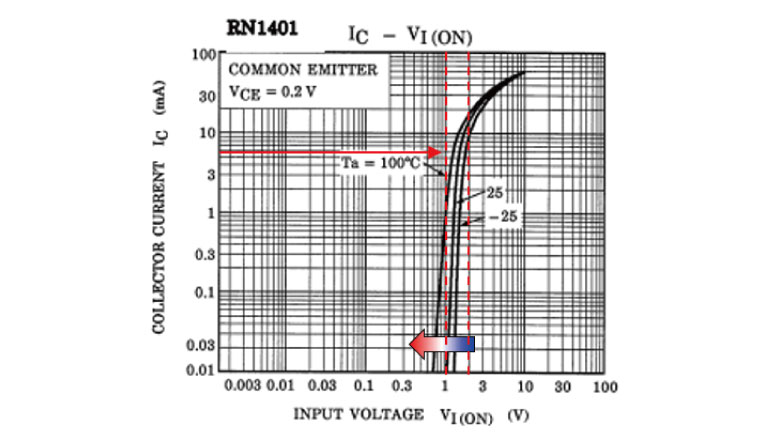
| 特性 | 符号 | 测试条件 | 最小值 | 典型值 | 最大值 | 单位 | |
|---|---|---|---|---|---|---|---|
输入电压(导通) |
RN1401 | VI(ON) | VCE=0.2V,IC=5mA |
1.1 | — | 2.0 | V |