
东芝推出适用于工业设备的100V大电流光继电器
2021年02月05日
东芝电子元件及存储装置株式会社
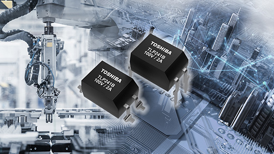
中国上海——东芝电子元件及存储装置株式会社(“东芝”)今日宣布,推出新款光继电器——“TLP241B”,该款大电流光继电器采用DIP4封装,适用于可编程逻辑控制器和I/O接口等工业应用。样品提供和量产现已开始。
TLP241B集成了基于东芝最新一代U-MOS工艺的MOSFET。使用TLP241B,断态输出端电压提高到100V,较当前TLP241A的40V提高了150%。该继电器采用通用型DIP4封装,是业界首款[1]可提供100V断态输出端电压,2A导通电流和5kV隔离电压的DIP4封装产品。该继电器在额定值提高之后可适用于多种类型的应用。
TLP241B可以取代常开型接触式机械式继电器。不同于机械式继电器,TLP241B没有会发生老化的触点。此外,它的低电流驱动特性还能延长产品使用寿命。它的其他优点是响应时间短,并且由于封装尺寸较小而节省了PCB空间。
由于最高额定工作温度为110℃,因此设备的温度设计裕度更容易获得。
应用
- 工业设备(可编程逻辑控制器、I/O接口和各种传感器控制等)
- 楼宇自动化系统(暖通空调(HVAC)和温控器等)
- 替代机械式继电器(交流24V至48V系统,直流24V至100V系统)
特性
- 高导通额定电流:ION=2A,IONP=6A(脉冲)
- 断态输出端额定电压:VOFF=100V
- 高额定工作温度:Topr max=110℃
- 提供鸥翼式封装(SMT)选项的通用型DIP4封装
主要规格
(除非另有说明,@Ta=25℃)
器件型号 |
||
|---|---|---|
封装 |
DIP4 |
|
绝对最大额定值 |
断态输出端电压 VOFF(V) |
100 |
导通电流ION(A) |
2.0 |
|
导通电流(脉冲)IONP(A) |
6.0 |
|
工作温度Topr(℃) |
-40至110 |
|
耦合电气特性 |
触发LED电流IFT 最大之(mA) |
3 |
导通电阻RON 典型之(mΩ) |
110 |
|
导通电阻RON 最大值(mΩ) |
200 |
|
电气特性 |
输出电容COFF 典型值(pF) |
300 |
开关特性 |
导通时间tON 最大值(ms) |
3 |
关断时间tOFF 最大值(ms) |
0.5 |
|
库存查询与购买 |
|
|
注:
[1] 在所有采用DIP4封装的光继电器中,截至2021年2月4日的东芝调研。
如需了解相关新产品在线分销商网站的供货情况,请访问:
TLP241B

客户问询:
日本总部
光电器件销售与市场部
电话:+81-3-3457-3431
中国地区
分立器件市场部(Discrete Marketing)
上海:021-6090-0610/深圳:0755-3661-5889
* 本文提及的公司名称,产品名称和服务名称可能是其各自公司的商标。
* 本文档中的产品价格和规格、服务内容和联系方式等信息,在公告之日仍为最新信息,如有变更,恕不另行通知。