
用于车载设备的小型MOSFET产品线中新增了40 V产品,其低导通电阻有助于降低功耗
产品新闻2022年3月
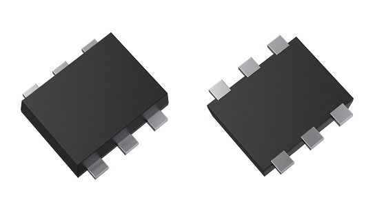
东芝电子元件及存储装置株式会社 (“东芝”) 推出了用于车载设备的40V N沟道MOSFET“SSM6K804R”,以扩充产品线。
新产品SSM6K804R采用新工艺制造,实现业界领先[1] 低导通电阻,4.5V栅源电压条件下,最大导通电阻为18mΩ。此外,扁平引线封装提高了芯片安装能力,降低热阻。产品采用小型TSOP6F封装,额定功耗仅为1.5W[2],有助于降低设备能耗。
与东芝同等额定功耗的SOP-8封装产品相比[3],TSOP6F封装产品安装面积约减小70%,有助于减小设备尺寸。此外,产品符合AEC-Q101标准,适用于车载DC-DC转换器等各种应用。
注:
[1]与TSOP6F级封装,具有相同最大额定值的产品进行比较,根据东芝调查(截至2022年2月)
[2]安装在环氧树脂板上(FR4,25.4mm×25.4mm×1.6mm,铜焊盘:645mm2)
[3]TP89R103NL等
应用
- 车载设备(反接保护、负载开关、DC-DC转换器等)
特性
- 业界领先[1]低导通电阻降低能耗:
RDS(ON)=18mΩ(最大值)@VGS=4.5V - TSOP6F封装降低了饱和热阻,额定功耗仅为1.5W
- 通过AEC-Q101认证
主要规格
(@Ta=25°C)
器件型号 |
极性 |
封装 |
绝对最大额定值 |
电气特性 |
||||||
|---|---|---|---|---|---|---|---|---|---|---|
名称 |
尺寸典型值 (mm) |
漏极-源极电压 VDSS (V) |
栅极-源极电压 VGSS (V) |
漏极电流 (直流) ID (A) |
功耗 PD (W) |
漏极-源极 导通电阻 RDS(ON) 最大值 (mΩ) |
输入电容 Ciss 典型值 (pF) |
栅极总荷电量 Qg 典型值 (nC) |
||
@VGS= 4.5V |
||||||||||
N沟道 |
TSOP6F |
2.9×2.8×0.8 |
40 |
±20 |
12 |
1.5 |
18 |
1110 |
7.5 |
|
30 |
15 |
12 |
1130 |
7.5 |
||||||
60 |
6 |
51 |
550 |
9.3 |
||||||
100 |
3.5 |
92 |
430 |
3.2 |
||||||
100 |
10 |
36.4 |
1110 |
8.5 |
||||||
注
[4]现有产品
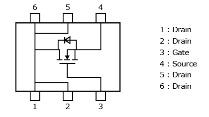
内部电路
应用电路示例
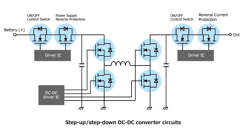
注:
本文所示应用电路仅供参考。
需要进行全面评估,特别是在量产设计阶段。
提供这些应用电路示例并不授予任何工业产权许可。
*本文档中的产品价格和规格、服务内容和联系方式等信息,在公告之日仍为最新信息,如有变更,恕不另行通知。