


Thermal Management for Designs Using Discrete Semiconductor Devices
There are several effective ways to manage the high temperatures of today’s discrete semiconductors in your design. Simulation techniques are vital for measuring how well each approach is working. This article introduces our thermal simulation results. We hope that this document will help you minimize heat generation problems when designing.
Introduction
It’s no surprise that semiconductor chip temperatures are trending upward. That heat can cause severe issues with performance and functionality. For example, Figure 1 illustrates the increasing need for surface-mount packages that exhibit optimal thermal performance.
There are various thermal design approaches that support the dissipation of heat, but which ones work best?
There are several causes behind the trend toward temperatures in discrete semiconductor devices rising. One is the reduced self-heat dissipation resulting from a reduction in the size of the electronics. Another cause is the increased ambient operating temperatures that come with high-density board assemblies. Furthermore, thermal heat generation has increased alongside efforts to achieve higher-speed operations.
■Contents
- Chapter 1: Design Countermeasures to Mitigate Heat Issues
- Chapter 2: Copper Trace Layers, TIM, and Vias
- Chapter 3: Simulating the Effects of Different Approaches
- Chapter 4: Modeling Vias and Heatsinks
- Chapter 5: Simulation Results
- Chapter 6: Toshiba Semiconductor Solutions
- Download PDF
- Related Links
Chapter 1: Design Countermeasures to Mitigate Heat Issues
There are several ways to mitigate temperature issues. For example, multi-layer PCBs will impact the thermal design of an electronic device because most of the heat generated is going to be dispersed by thermal conduction to the top and bottom surfaces and the internal structures of the PCB. Increasing the number of layers is a proven way to increase power dissipation. However, this is primarily effective when 4 to 8 layers are used and will impact the cost.
Heatsinks mounted directly on the PCB are one way to dissipate the heat generated by components on the PCB board. However, the amount of dissipation is directly related to the heatsink size and the heatsink emissivity.
While increasing the size of a heatsink seems like an extremely effective approach to dissipating heat, it must be balanced with size and cost constraints. Measures taken to enhance heatsink emissivity, such as surface treatments with anodized aluminum, are also quite effective but again limited by cost.
Reference links:
Chapter 2: Copper Trace Layers, TIM, and Vias
Using copper trace layers significantly increases the thermal conductivity of the board itself. Furthermore, increasing copper trace thickness further increases the surface area from which heat can be effectively dissipated, thus enhancing the overall thermal conductivity of the board.
Thermal interference is particularly noticeable when multiple heat-generating devices are arranged in a row. If the devices are too close together, heat generation is more problematic. And while spacing the devices further apart will help, there is a distance at which no more gains to be achieved. Another factor is the TIM (Thermal Interface Material). The use of a thinner TIM will assist in more effective dissipation but is more challenging to optimize when using TIM for a small surface area.
Vias are holes in the PCB to establish electrical connections between layers of a printed circuit board. Vias just below a drain frame are quite effective at dissipating heat. Meanwhile, peripheral vias, while not as efficient, do work well at preventing the conduction of heat to surrounding areas.
Chapter 3: Simulating the Effects of Different Approaches
Not all of these methods described above are equal in their ability to address heat generation issues, and their effectiveness may vary significantly depending on the design conditions. Because of this, we performed simulations to evaluate how well each of these thermal design approaches worked and what parameters produced the best results.
More details about the model and simulation specifics can be found in the application note Discrete Semiconductor Devices Hints and Tips for Thermal Design ̶ Part 2. Note that one of the most powerful benefits of these simulations was the opportunity to use models and conditions that are impossible to achieve with physical measurement.
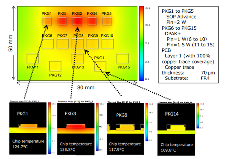
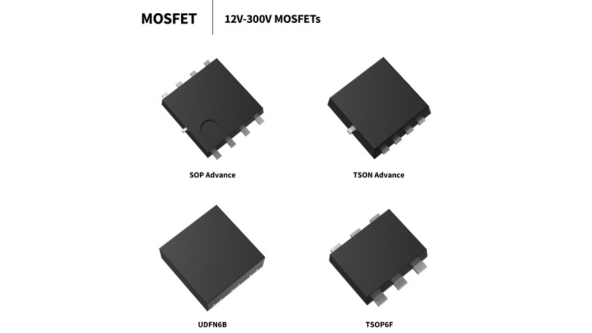
The device model for this thermal design evaluation is shown in Figure 2 below and uses SOP Advance, TSON Advance, and DSOP Advance chip packaging.

The PCB was modeled as a 2-inch square, and only the solder resist on the backside was modeled. The solder resist present on the front side was simulated by increasing the emissivity of the board material (for example, glass epoxy FR4). This approach was strategically chosen to reduce the density of the surface mesh while maintaining the same effect as a solder resist.
This PCB thickness was approximately 1.6 mm, based on the most commonly used PCBs. The standard PCB used in the simulation was modeled with four layers, copper was used for the trace material, and all copper trace thicknesses were set to 70 μm for evaluation.
Reference links:
Chapter 4: Modeling Vias and Heatsinks
Vias were modeled as thermal through-holes, were 0.25 mm square, and placed on the drain trace that serves as the primary thermal path in the package. Vias placed on a copper trace just below were modeled as inner vias; those around the periphery served as outer vias. A heatsink with the same shape and modeled using cuboids was used for all simulations except when it was parameterized.
For the thermal interference model, three instances of a device were placed on the common drain trace and used a PCB with the same size as for a single-device simulation described earlier.
For all models, the same physical property values were used for the TIM, and only its thickness was via. The effect of TIM was evaluated by placing it (1) between a copper trace and a device and (2) between a copper trace and a heatsink.
Chapter 5: Simulation Results
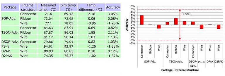
As shown in Figure 3, the accuracy of the simulation was found to be within an acceptable range of ±5 %.
5-1: Multi-layer PCBs
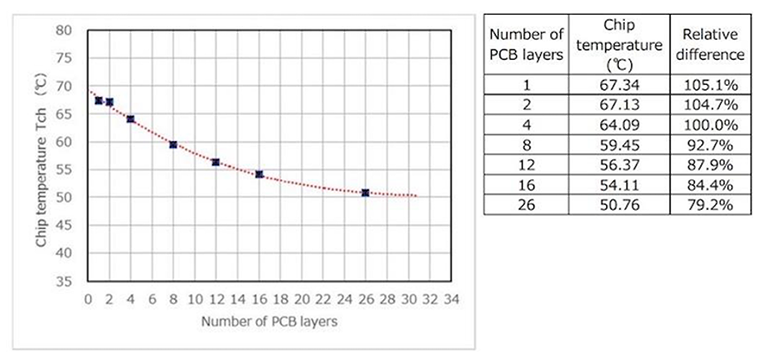
The effects of multi-layer PCBs are illustrated in Figure 4. Simulation results showed that the chip temperature was reduced by 7 % when the number of PCB layers was increased from 4 to 8. The primary issue lies in the increased cost.
5-2: PCB Trace Thickness
Increasing the trace thickness from 70 μm to 105 μm reduced chip temperature by 6 %,
5-3: Heatsink Size
For a design with no heatsink, adding a 1 cm tall heatsink dropped the chip temperature by 12 %. When a heatsink with a height of 2 cm was modeled, it resulted in a 19 % reduction in board temperature. This particular approach is much more effective than depending solely on the PCB to dissipate heat.
5-4: Heatsink Emissivity
The emissivity of a heatsink can be increased from 0.04 to 0.8 by treating the surface with anodized aluminum. When such a heatsink was implemented, it decreased chip temperature by 12 %. While extremely effective, this surface treatment can significantly impact the cost.
5-5: Thermal Interference
For three devices in a row, a spacing of 3 mm caused a 3 % increase in chip temperature; however, there was no increase in temperature when a spacing of 12 mm was implemented.
5-6: TIM
For a small surface area, benefits are to be gained from using a thinner TIM; this is not true, however, when larger surface areas are involved.
5-7: Vias Just Below a Drain Frame
Placing vias just below a drain frame proved quite effective when compared to a PCB with no via. A 9 % chip temperature drop was achieved when three vias were added, and adding five vias resulted in a 12 % temperature drop.
5-8: Peripheral Vias
When compared to a PCB with no via, adding six vias led to a 7 % drop in chip temperature, while ten vias resulted in a 10 % temperature drop. It is worthy of note, however, that peripheral vias were less effective than vias placed just below a drain frame. On the other hand, peripheral vias do have an excellent benefit to their use: they may prevent the conduction of heat to surrounding areas.
Chapter 6: Toshiba Semiconductor Solutions
Not all surface mount packages are created equal when it comes to thermal design and performance, which is why we have actively pursued the development of solutions that provide superior thermal performance in their packaging, including MOSFET packages, the SOP Advance package, and the TO-247 package used in the simulation.
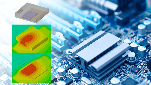
We have semiconductor components with cutting-edge packaging that implements the proven methods just discussed. Also, we offer you a simplified 3D model (simplified CFD model) suitable for the thermal simulation, focusing on MOSFETs, to help you better understand the temperature distribution of your design and find effective methods of minimizing temperature.
Reference links:
Download PDF
Please click the button to download the PDF file.
Related Links
To learn more about thermal design, please see the PDF article below.