What are the power semiconductors that will create a carbon-neutral future?
We Toshiba Electronic Devices and Storage Corporation contribute to the realization of a future carbon neutral world. By realizing high-performance power semiconductors with the latest technology. By accelerating energy conservation in all types of electrical equipment.
What is Power Semiconductor?
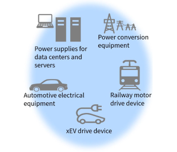
Semiconductor device that controls the flow of electricity to reduce power loss. Personal computers and other electronic equipment constantly lose power when they operate. Power loss can be kept low by using high performance power semiconductors. High performance power semiconductor can realize saving energy for not only Personal Computers, but also Smartphones, Automotive application, Trains, and Electrical substations. Our high performance power semiconductor contributes to realize of a future carbon neutral world!
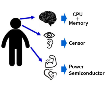
Heart or Muscle if human-being
Efficient control of electric power
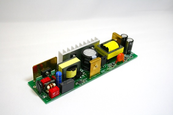
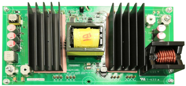
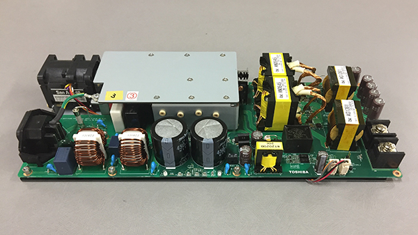
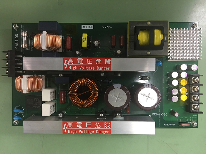
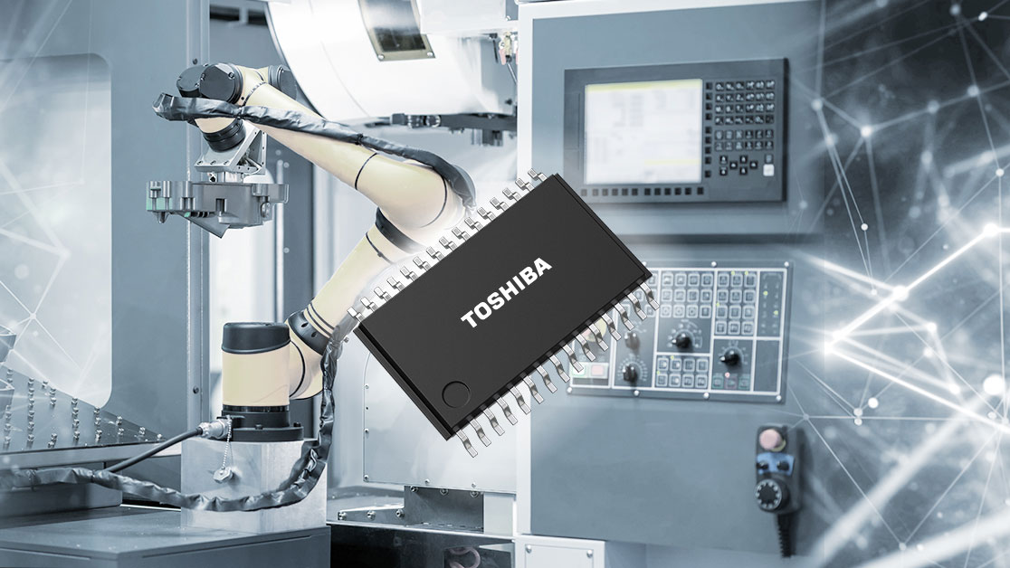
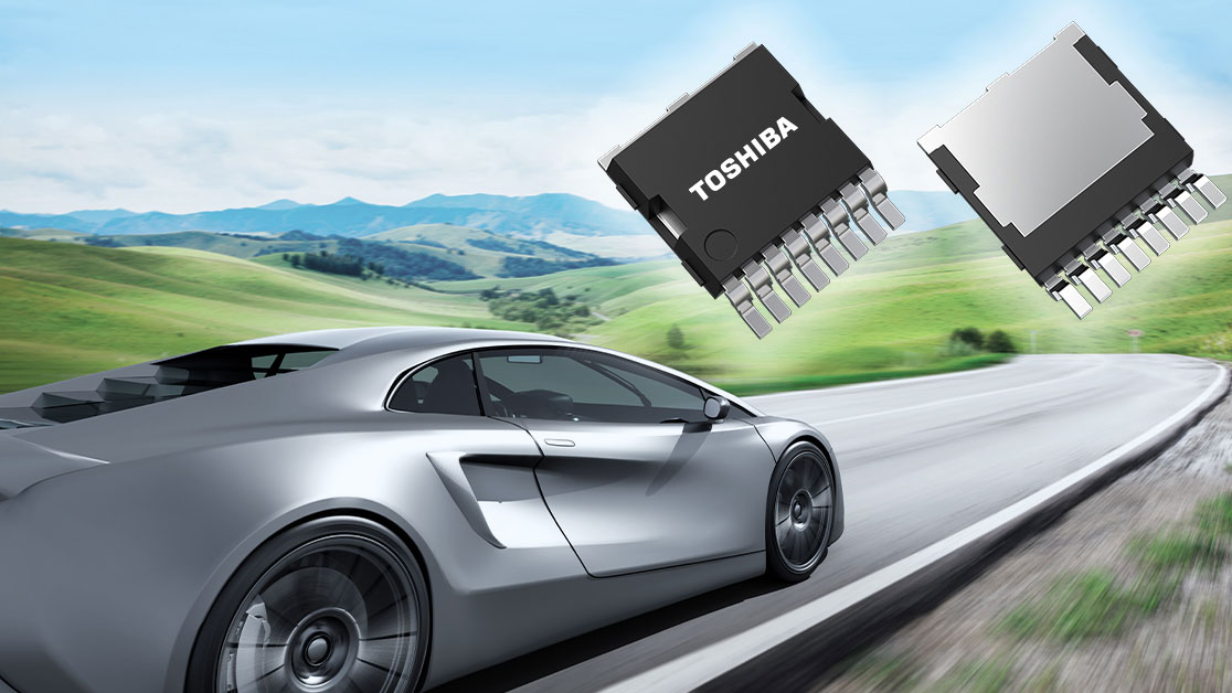
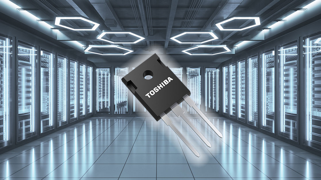
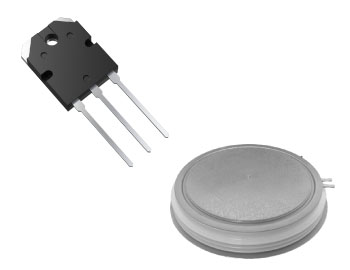
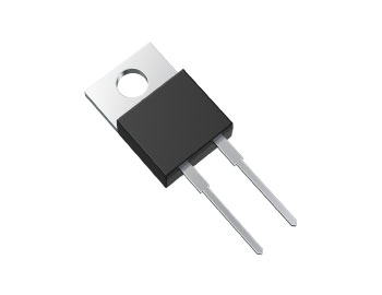
Power Semiconductor Example
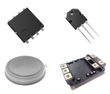
Toshiba Electronic Devices & Storage Corporation’s Power semiconductor
We provide customers with various types of Power Semiconductor. To reduce the power loss in all electric equipments around the world.
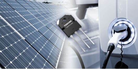
While energy conservation is attracting attention to realize a decarbonized society, demand for electricity is increasing, so there is a rapidly growing need for smaller power converters with low power loss. As a result, not only improvements in the performance of Si power devices, but also the introduction of Wide-bandgap (WBG) Semiconductor is under way. We are expanding our product lineup of Si power devices and expanding our manufacturing facilities. For WBG Semiconductor, we have commercialized Silicon Carbide (SiC) power semiconductor. We are also developing Gallium Nitride (GaN) power semiconductor.

[Note 1] IEGT: Injection Enhanced Gate Transistor
[Note 2] Diodes: include products other than power semiconductors
e-Learning
You can see the video from “What is Semiconductor?” to the “Fundamental of Power Semiconductors”.
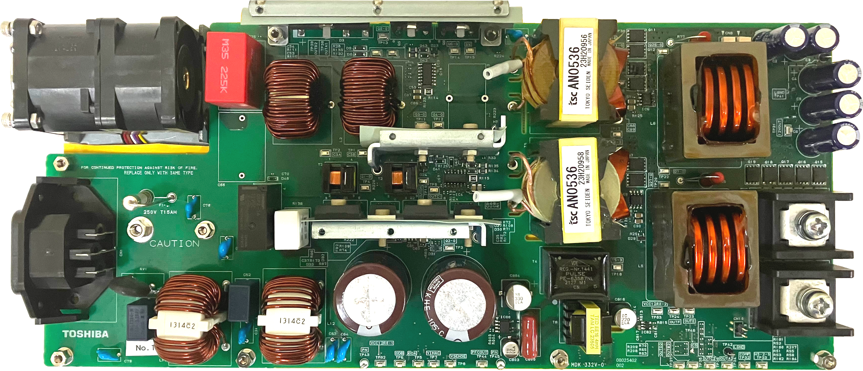
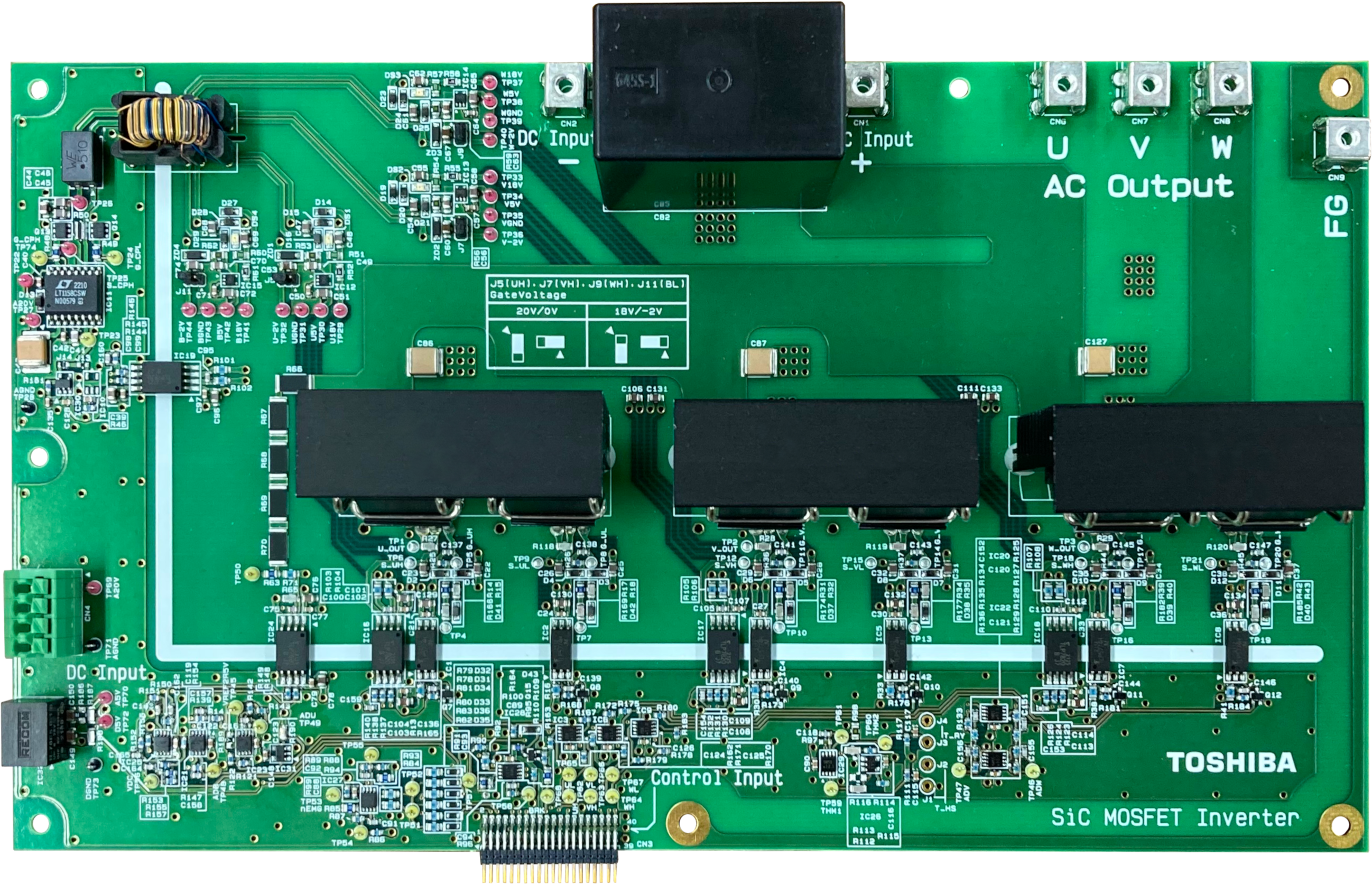
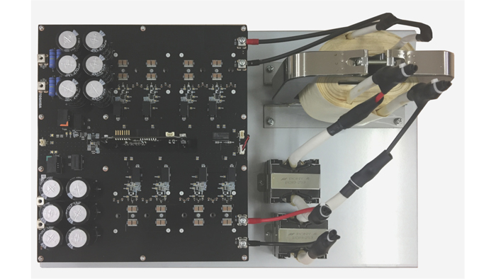
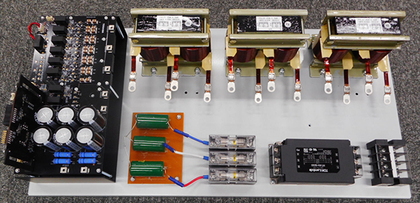
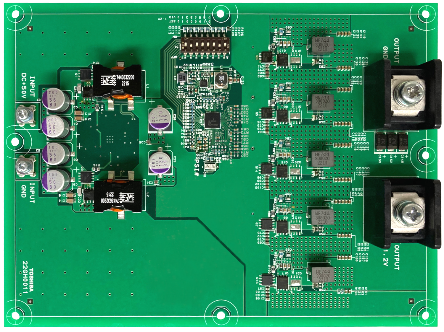
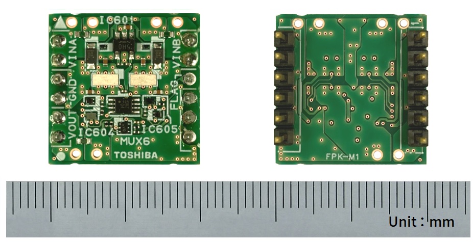
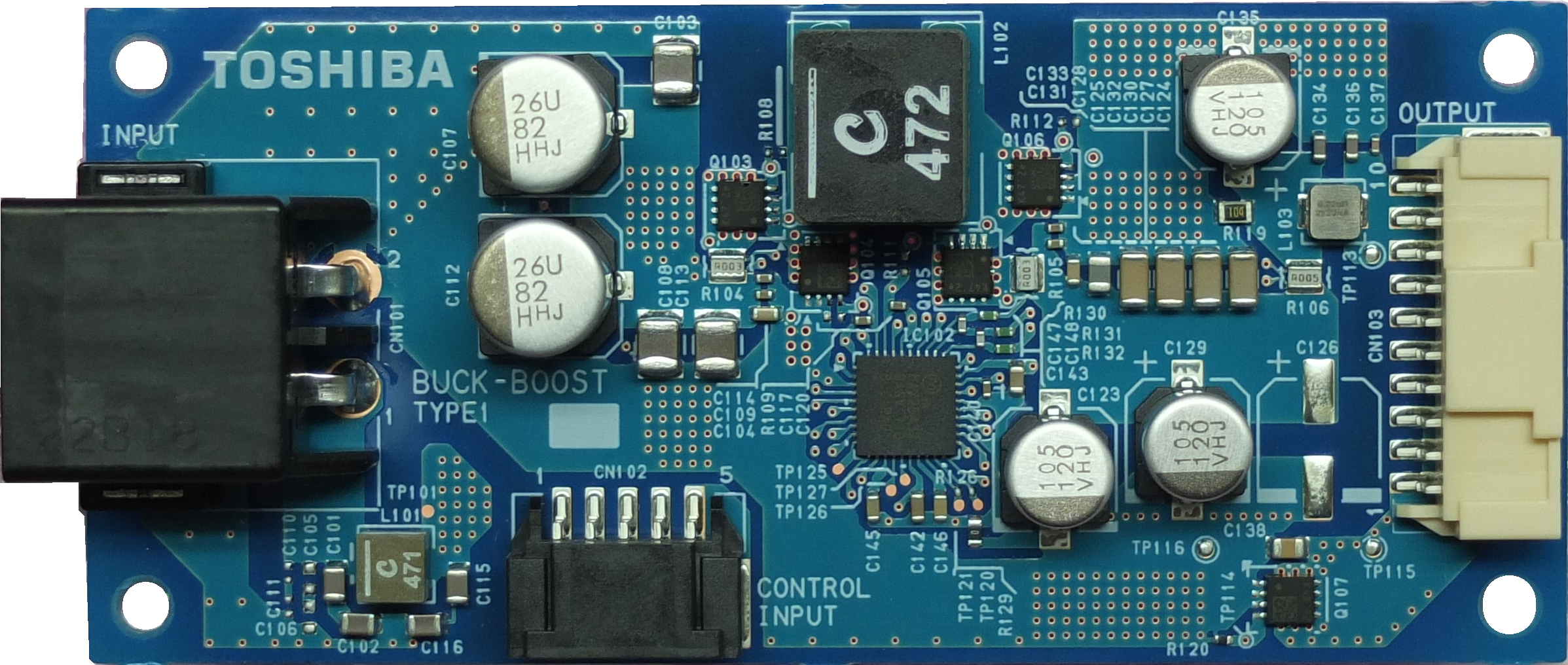
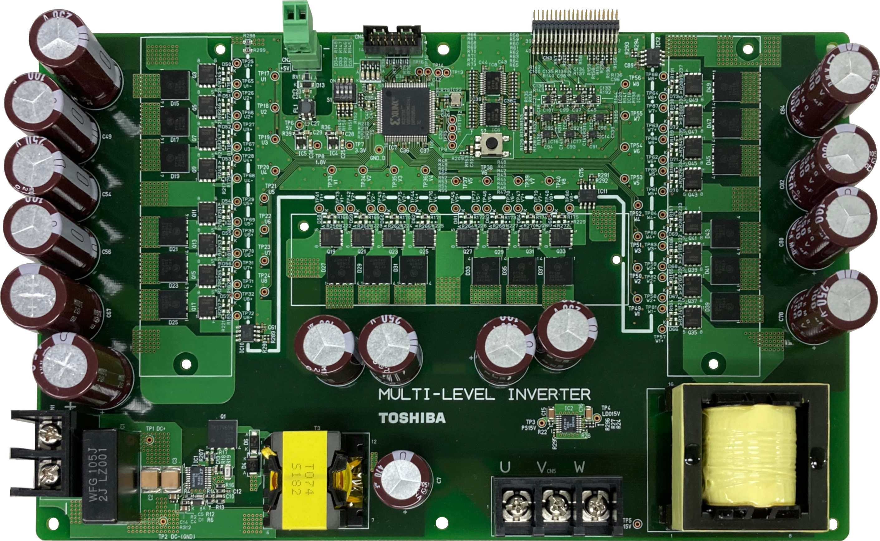
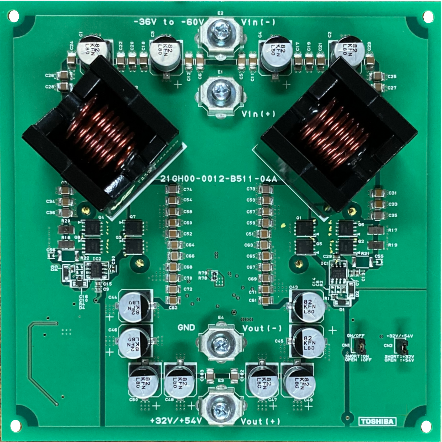
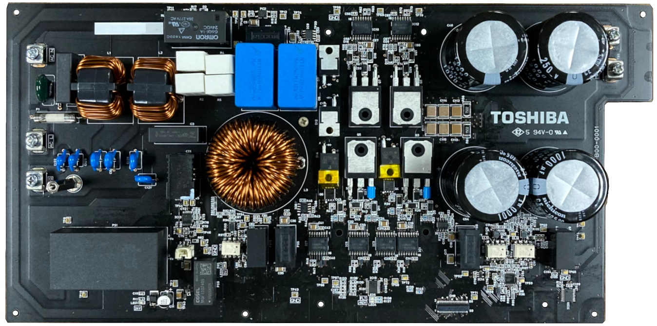
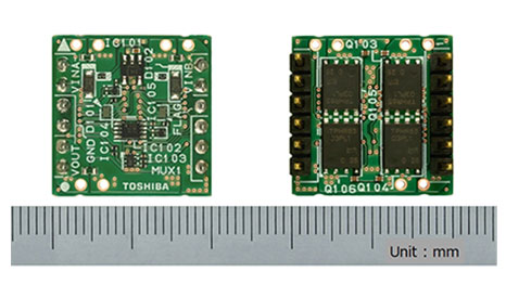
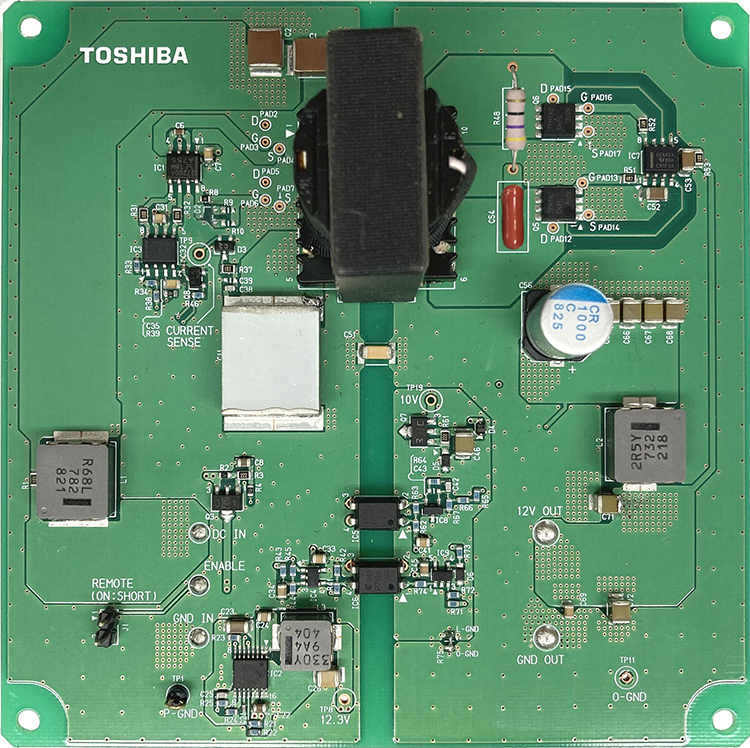
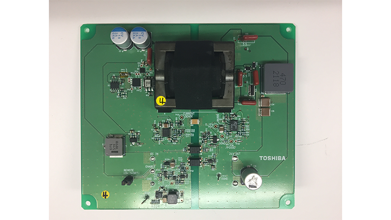
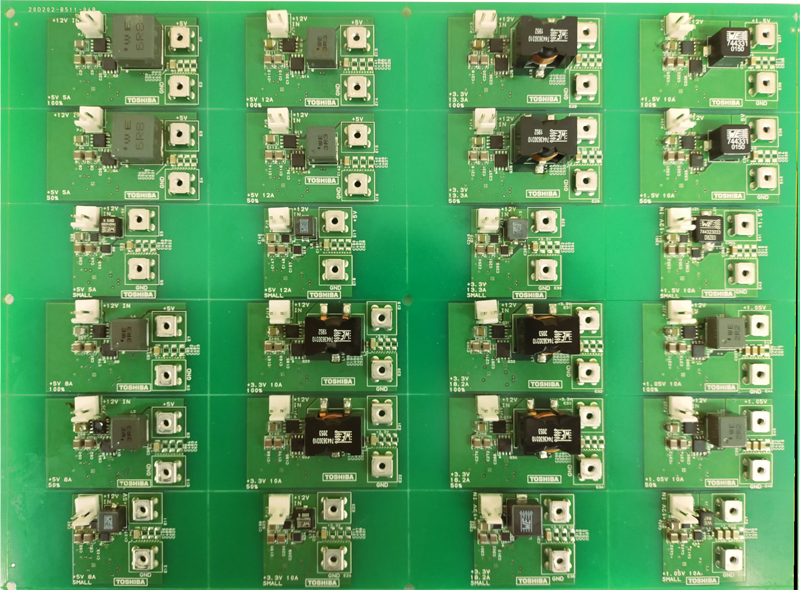
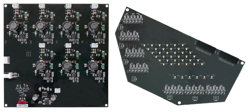
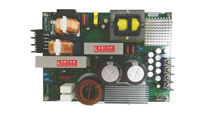
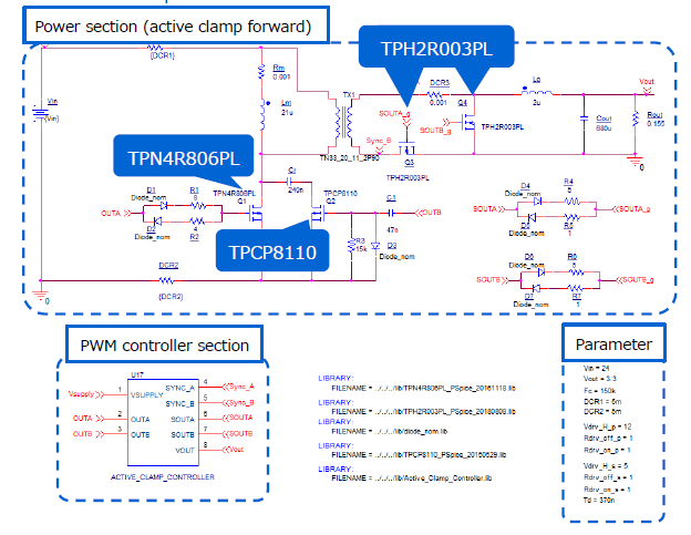
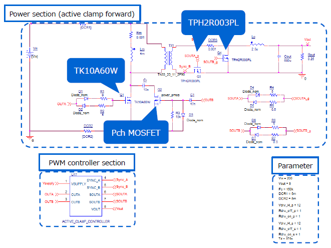
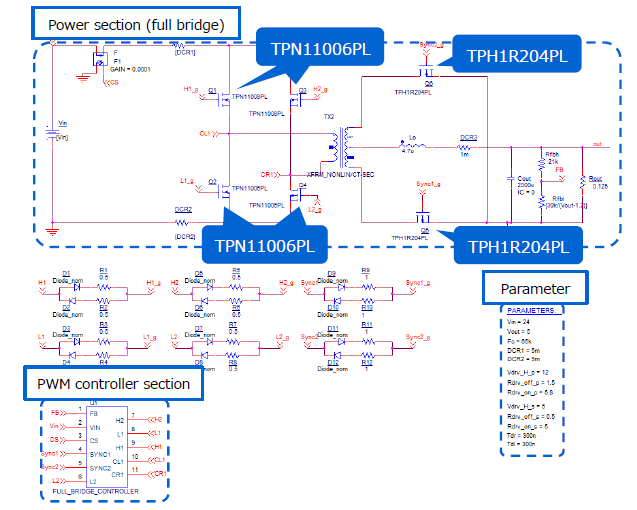
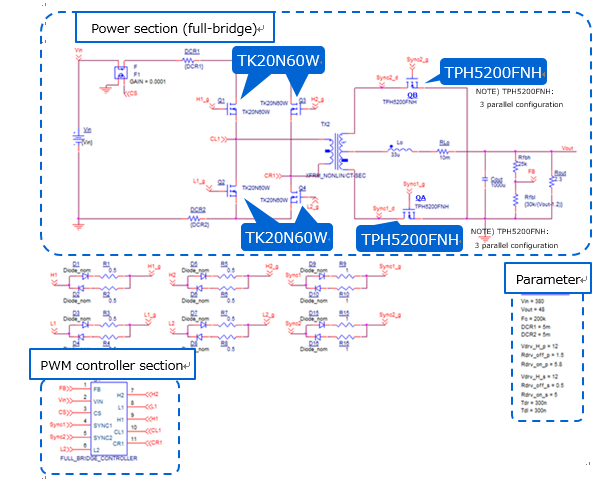
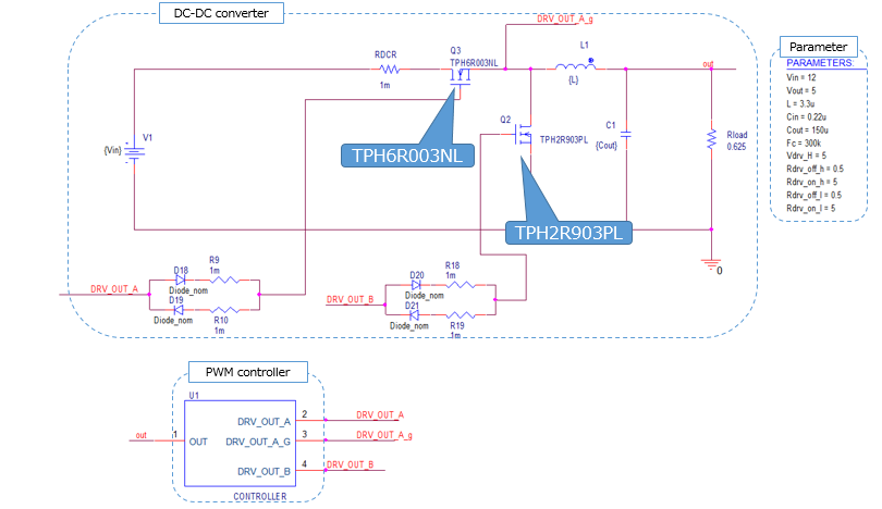
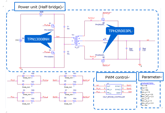
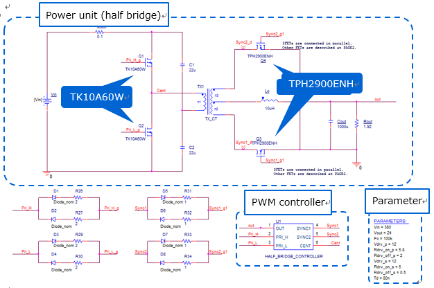
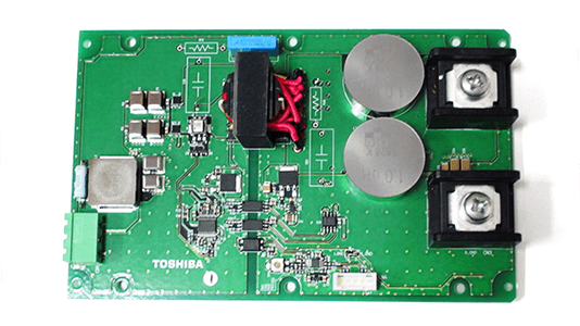
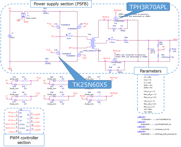
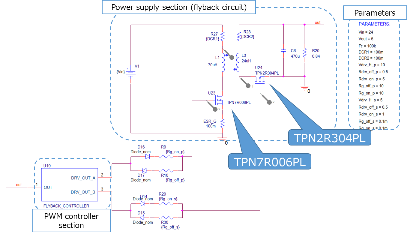
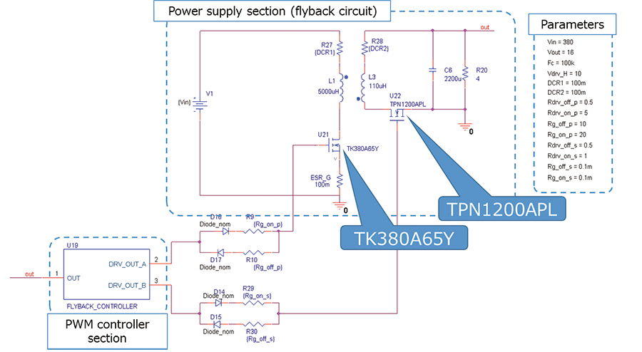
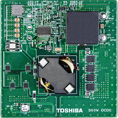
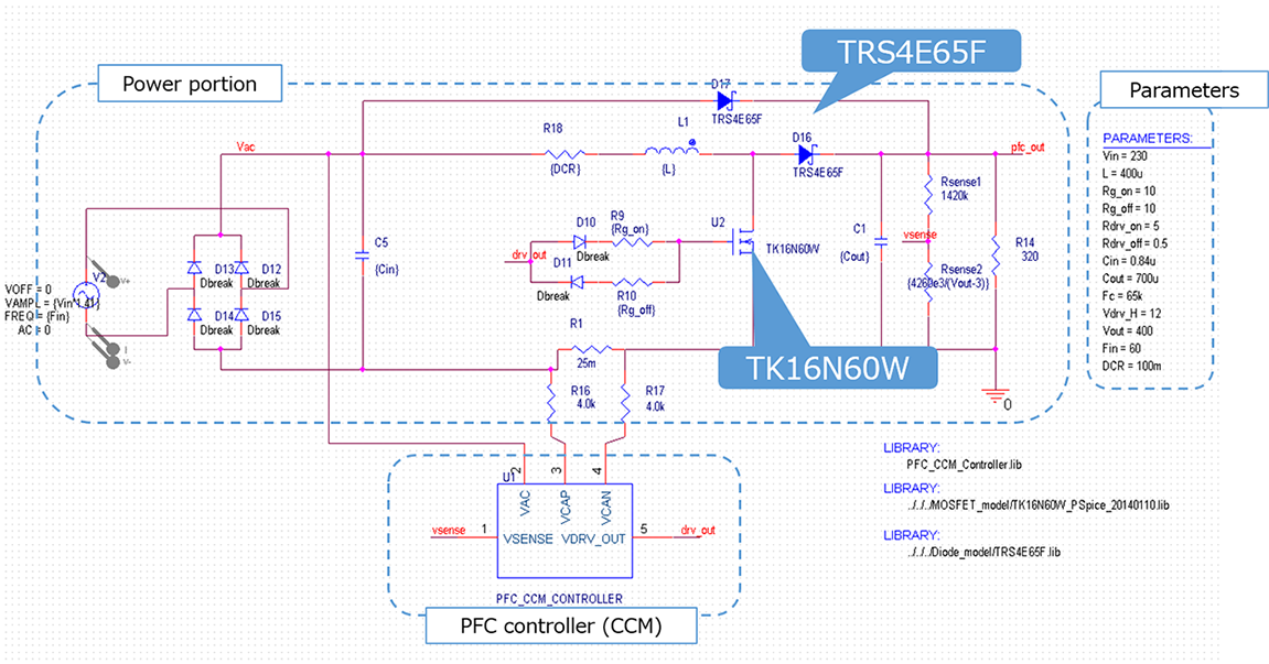
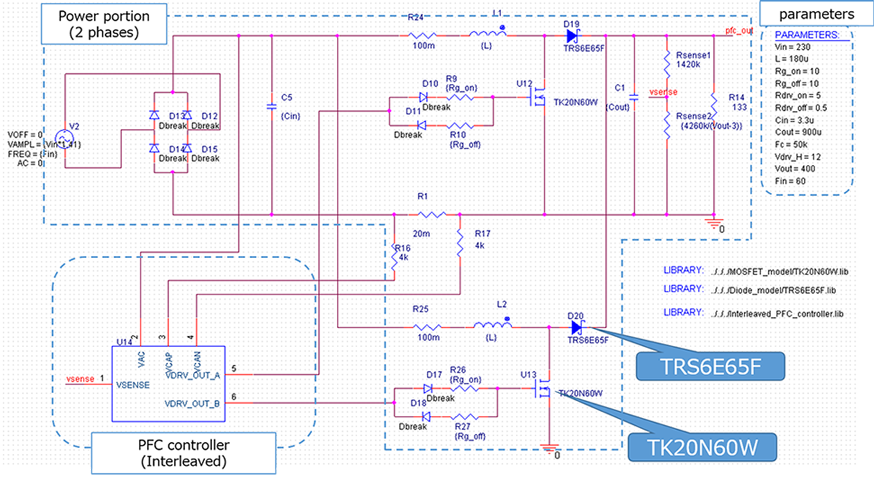
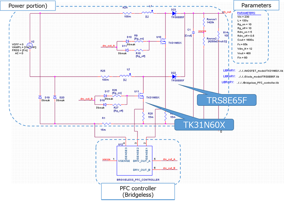
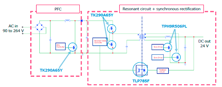
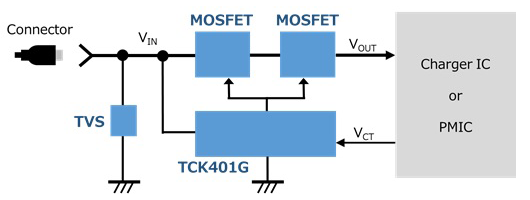
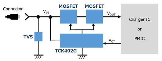
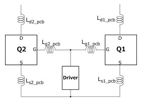
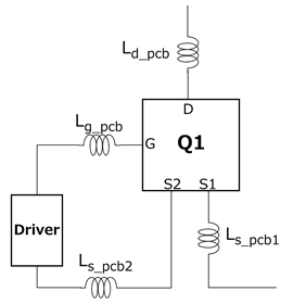
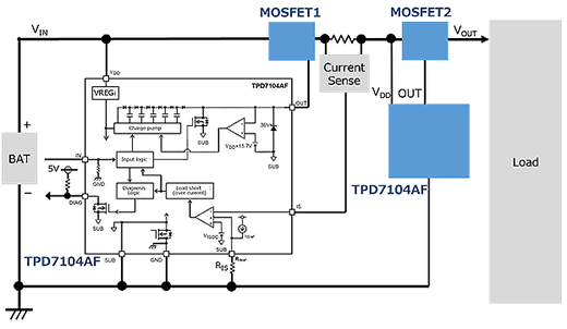
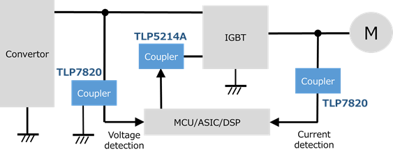
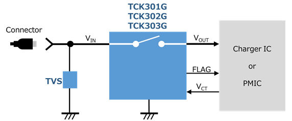
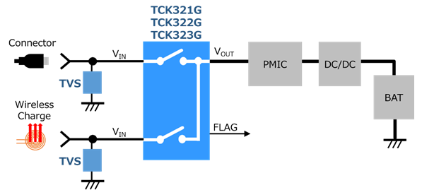
Reference Design