


Efficiency Improvement by Multi-Level Inverter with 150 V MOSFET
Inverter to control motors is necessary for industrial robotic applications that contribute factory automation.
We introduce the approach of multi-level inverter method with 150 V MOSFET on behalf of 2-level inverter method with 600 V MOSFET to improve efficiency.
- Able to finer output voltage control using the multi-level inverter compared to using the 2-level inverter
- Realization of efficiency improvement with 150 V MOSFET which has lower on-resistance and lower gate charge than 600 V MOSFET has
- Provides reference design which can support 5-level operation
* There are several types of multi-level inverters in this industry. Diode clamp type NPC (Neutral Point Clamp) multi-level inverter is called “MULTI-LEVEL INVERTER” here.
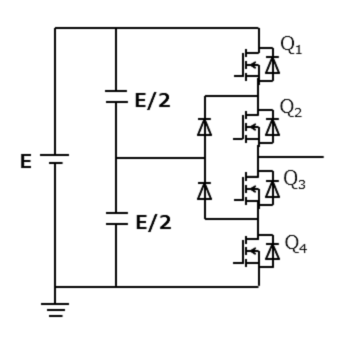
Multi-Level Inverter

The multi-level inverter which contains multiple switching devices in series on a switching portion, that a general inverter (2-level inverter) contains one switching device on, is able to control output voltage finely.
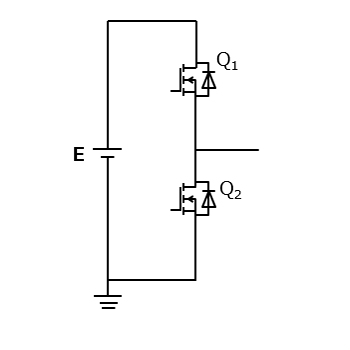
Fig.1 shows a block diagram of bridge circuit which is a part of general 2-level inverter circuitry. (The inverter circuitry consists of multiple numbers of this portion depending on a motor to be controlled. A 3-phase inverter to control a 3-phase motor consists of 3 pieces of bridge circuit.) In this figure, 2 switching devices (MOSFET is used in this figure), Q1 and Q2, are located between voltage source and ground, and desired voltage is output through midpoint by controlling ON/OFF of Q1 and Q2. (The portions between voltage source and midpoint, and between midpoint and ground where one MOSFET is located are called “arm”.)
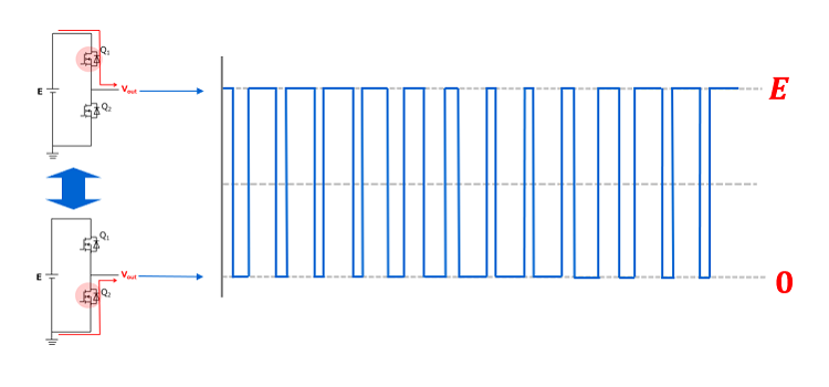
As a 2-level inverter operation waveform shown in Fig.2, the output voltage has 2 levels, E (voltage source voltage) when Q1 is ON and Q2 is OFF, and 0 (ground voltage) when Q1 is OFF and Q2 is ON.
The 2-level inverter has one switching device in each arm, but the multi-level inverter has multiple switching devices in each arm. Desired voltage is output through midpoint by controlling each switching device. We explain operation of a 3-level inverter which has 2 switching devices in each arm which is shown in Fig. 3 as an example.
Fig.4 shows a 3-level inverter operation example. Three periods, when Q1 and Q2 is ON, when Q2 and Q3 is ON, and when Q3 and Q4, are repeated. The output voltage has 3 levels, E when Q1 and Q2 is ON, E/2 when Q2 and Q3 is ON, and 0 when Q3 and Q4 is ON. In this way, the 3-level inverter has an advantage that output voltage can be controlled finely because of sesquialteral output voltage resolution.
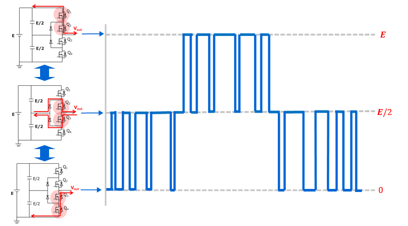
Now, we consider output volage amplitude and applied voltage to each switching device of 2-level inverter or 3-level inverter when both voltage source voltage is E. Output voltage amplitude of the 2-level inverter is E because output voltage has E and 0, then applied voltage to each device is also E. On the other hand, output voltage amplitude of the 3-level inverter is E/2 because output voltage has E, E/2 and 0, then applied voltage to each device is also E/2. Therefore, in the 3-level inverter case, the applied voltage to each switching device becomes half compared with 2-level inverter and half withstand voltage device may be used. In general, switching operation power loss of switching device such as MOSFET becomes worse as its withstand voltage increases because its on-resistance per unit area increases. Thus, using lower withstand voltage device contributes to reduce power loss of applications with multi-level inverter.
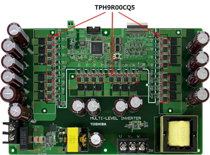
TPH9R00CQ5 Application to Multi-Level Inverter
Newly released TPH9R00CQ5 is a 150 V MOSFET which realizes to reduce switching operation power loss because it is optimized cell structure using the latest U-MOSX-H process and the trade-off between the on-resistance and the charge characteristics is improved well compared with our older generation products. This is a high speed diode (HSD) type product whose internal diode speed is gained by life time control technology and is suitable for inverter applications that free wheel current at motor driving flows through its internal diode other than switching power supply applications as well.
We discuss the multi-level inverter which this TPH9R00CQ5 applies to. If inverter output is assumed 3-phase AC 200 to 240 V, the input voltage needs around DC 400 V. In 2-level inverter case, 600 V or above withstand voltage would be used in consideration of surge voltage at switching operation although applied steady state voltage amplitude to the switching devices is 400 V. If the TPH9R00CQ5 is used, 5-level inverter which contains 4 devices in series will be sufficient.
Now, we compare a switching device on 2-level inverter to TPH9R00CQ5, which is used on 5-level inverter, in characteristics for switching applications point of view. As we mentioned above, withstand voltage of the switching device on 2-level inverter needs 600 V or above, thus TK62N60W5 (600 V/DTMSOIV/HSD type) which is suitable for inverter application because of built-in high speed diode and 600 V withstand voltage was selected. In the TPH9R00CQ5 case, total characteristics of 4 devices are considered when the TPH9R00CQ5 characteristics are compared to the TK62N60W5 characteristics because the TPH9R00CQ5 is used on the 5-level inverter. Table 1 shows on-resistance (RDS(ON)) values which affect conduction loss when current applies and gate charge (Qg) values which affect switching loss when MOSFET turns ON/OFF of two devices, TPH9R00CQ5 and TK62N60W5. As shown on Table 1, TPH9R00CQ5 (4 devices total) has smaller value on both on-resistance and gate charge than TK62N60W5 has. This indicates that the 5-level inverter with TPH9R00CQ5 will have lower power loss compared to the 2-level inverter with TK62N60W5 if those inverters operate.
Table 1 Characteristics Comparison TPH9R00CQ5 (4 devices total) and TK62N60W5
| 5-level inverter (TPH9R00CQ5, 4devices total) |
2-level inverter (TK62N60W5) |
|||||||||
| RDS(ON) (@VGS = 10 V) | 36 mΩ (9 mΩ x 4) | 45 mΩ | ||||||||
| Qg (VGS = 0~10 V) | 176 nC (44 nC x 4) | 205 nC | ||||||||
Reference Design Outline
New approach of multi-level inverter with 150 V MOSFET on behalf of 600 V MOSFET
- Input: DC 400 V (Max.)
- Rated output : 3-phase AC 200 to 240 V, 10 A
- Control power : DC 5 V
- Up to 5-level operation available
Related link
Follow the links below for application information using 150 V MOSFET
Inverter/Servo
Follow the links below for various reference designs that can be used for end equipment design
Reference Design Center
We provide simulation data, 3D models of packages, and land pattern models (2D models) used when developing product boards.
EDA/CAD Model Library