


1.2. Internal operation of an op-amp
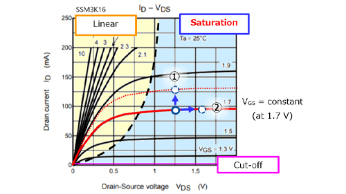
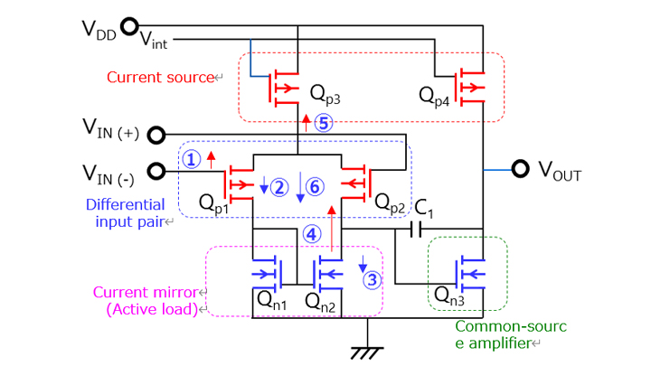
Figure 1-2 shows a simplified equivalent circuit for an op-amp. As you see, it is composed of multiple MOSFETs. For a CMOS op-amp to work properly, these MOSFETs need to operate in the saturation region. Figure 1-3 shows the saturation region of the MOSFET.
In this region, the MOSFET operates as follows:
- As the gate-source voltage increases, the drain current increases.
- As the drain-source voltage increases, the drain current increases slightly.
A slight change in drain current causes a considerable change in drain-source voltage.
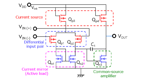
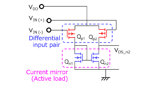
The portions of the op-amp provide the following functions:
- Differential input pair: Amplifies a difference in voltage between the VIN (+) and VIN (-) inputs
- Current mirror: Provides an equal amount of current to Qp1 and Qp2 comprising the differential input pair. The current mirror acts as load resistance for the differential input pair. Typically, the output of the current mirror (i.e., the drain terminal of the differential input pair) has high impedance, which is difficult to obtain with a typical resistor. As a result, the first-stage differential amplifier has a high gain. Such a resistive load composed of transistors is called an active load.
- Current source: Determines the amount of current that flows to the differential input pair and the common-source amplifier. The current source acts as an active load for the common-source amplifier.
- Common-source amplifier: Provides the drive current for an external load connected to the output and compensates for the gain of the first-stage differential amplifier
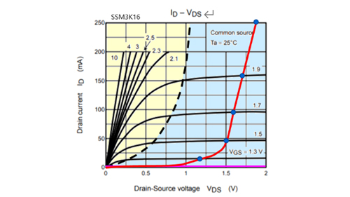
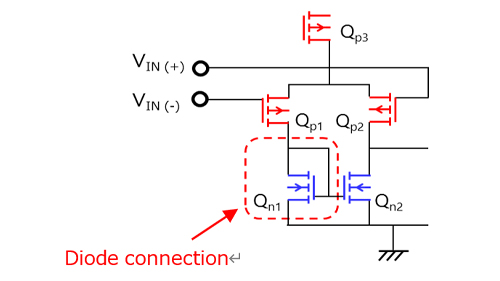
Before going into the operation of an op-amp, let’s discuss the drain voltage of Qn1 in the current mirror.
The drain-source voltage (VDS_n1) and the drain-gate voltage (VDG_n1) of Qn1 are equal. Figure 1-4 plots the conditions under which VDS = VDG is satisfied. Since the resulting curve looks like the IF-VF curve of a diode, the connection of Qn1 is called a diode connection. In Figure 1-4, the drain current is large because it is the ID-VDS curves of a discrete N-channel MOSFET with a large channel area. The internal MOSFETs of an IC have a drain current two to three orders of magnitude lower than this.
As Figure 1-4 indicates, after the drain current exceeds a certain point (at a VDS of 1.5 V or higher), a slight change in the drain current hardly affects the drain-source voltage.
Next, let’s consider how the current source works. First, let’s consider a circuit without a current source as shown in Figure 1-6. The subsequent common-source amplifier is identical to that of the previous op-amp.
An equal voltage (VDD – VIN) is applied to the differential inputs, VIN(+) and VIN(-). Hence, VSG = VIN. At this time, when the drain current (ID_p1) is conducted, the drain voltage of Qp1 settles to a voltage at which VSD_p1+VDS_n1=VDD. Since ID_p1 is copied by the current mirror, the circuit composed of Qp2 and Qn1 has the same voltage relationship as this.
Suppose that the voltage applied to VIN(+) and VIN(-) increases by ΔV to (VDD – VIN + ΔV). Since the circuit of Figure 1-6 has a current mirror, the same amount of current flows to the differential input pair. However, without a current source, the currents flowing to the differential input pair decrease by the same amount. As a result, the drain-source voltage of Qn2 connected to the common-source amplifier also decreases.
This is equivalent to a decrease in the gate-source voltage of Qn3 (VGS_n3) of the common-source amplifier. The common-source amplifier has a current source (Qp4), which raises the drain-source voltage (VDS_n3) to oppose a decrease in VGS_n3, keeping the current constant. In other words, the output voltage (VOUT) increases even though the VIN(+) and VIN(-) inputs have the same voltage and phase. It is essential that the op-amp have a constant output when a common-mode input (same input voltage) within the range shown in the datasheet is applied to VIN(+) and VIN(-). The circuit of Figure 1-6 cannot satisfy this requirement.
Next, let’s consider the circuit of Figure 1-2 with a current source (Qp3). Suppose, for example, that the input voltage applied to VIN(-) and VIN(-) increases by ΔV to (VDD – VIN + ΔV). Since this circuit has a current source, the current flowing to the differential input pair remains unchanged. Therefore, the drain-source voltage of Qn1 (VDS_n3) remains unchanged. Likewise, VDS_n2 remains unchanged. Therefore, the output voltage is constant for the common-mode input voltage.
(The VSD_p3 of Qp3 compensates for ΔV. The current flowing to the differential input pair changes because the source-drain voltage of the current source changes. Since the drain-source voltage of the current source changes, the drain current (ID) changes. However, ID changes only slightly with VDS. Therefore, ID does not change significantly.)
So, the role of the current source is to keep the output voltage constant when the common-mode input voltage is applied to VIN(+) and VIN(-).
Next, let’s consider the case in which different voltages are applied to VIN(+) and VIN(-).
- Suppose that VIN(+) and VIN(-) initially have the same voltage (VDD – VIN) and then the VIN(-) voltage increases by ΔV.
- VSG_p1 decreases, causing ID_p1 to decrease by ΔIp1. However, as explained above, Qn1 has a diode connection. Therefore, VDS_n1 remains unchanged. So, the drain voltage of Qp1 remains constant.
- The current mirror copies the decreased ID_p1 to the drain current of Qn2 (ID_n2).
- This is contradictory since the drain current of Qn3 (ID_p3) in the current source remains unchanged. Therefore, the drain voltage of Qn2 (VDS_n2) increases to increase the current flowing through Qn2.
- You might think that an increase in VDS_n2 causes VSD_p2 to decrease, causing ID_p2 to decrease. Note, however, that the current from the current source (ID_p3) remains unchanged. Since ID_p1 has decreased by ΔIp1, ID_p2 should increase, not decrease. Therefore, the source voltage of Qp2 increases.
- The source-gate voltage of Qp1 (VSG_p1) increases, causing its drain current (ID_p1) to increase.
- ID_p1 is copied to the drain current of Qn2 (ID_n2). Then, the operation returns to Step 3.
Eventually, the drain voltage of Qn2 (VD_n2) increases from the initial voltage.
The increased VD_n2 is transferred to the subsequent common-source amplifier.
The VGS_n3 of the common-source amplifier increases, causing ID_n3 to increase. However, the increase in ID_n3 is constrained by Qp4 of the current source. Since the increase in VGS_n3 does not lead to an increase in ID_n3, the drain-source voltage of Qn3 (VDS_n3) decreases.
This means that when the VIN(-) voltage increases, the VOUT voltage decreases.
Related information
- Prev
- 3/3
Chapter1 What is an op-amp?
Related information
- Products
- Application Notes
- FAQs
- Parametric Search
- Stock Check & Purchase